
Ultra wideband detectors developed with flat responses for high data rate ASK demodulation contain three blocks; an impedance conversion network (ICN), a diode and a lowpass filter (LPF). Wideband properties are achieved by designing the LPF to have a suitable input impedance in the stopband; and, high data rate capabilities are achieved by designing the ICN to have an appropriate output impedance at baseband frequencies. The ICN is also tuned by EDA tools to obtain a flat response. Measurements show narrowband fluctuations within 1 GHz of better than 1.07 dB in a 6 to 26 GHz band. The designed demodulation rate is 2.5 Gbps.

Figure 1 Conventional detector.
Detectors are used in microwave and millimeter wave circuits and systems to perform various functions such as power detection and signal demodulation.1 For demodulation, systems often employ amplitude shift keying (ASK), which is simple and capable of high data rates. Unlike detectors with high load impedances used for power detection or even low data rate demodulation, high data rate demodulation detectors usually require 50 Ω load impedances to facilitate post amplification.
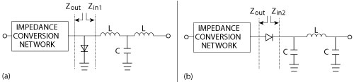
Figure 2 Two detector configurations; shunt (a), series (b).
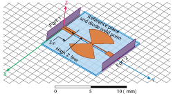
Figure 3 Microstrip realization of a LPF for the shunt detector.
For communication circuit engineers, research on demodulation detectors is still an active area; especially for optical, UWB or millimeter wave communication system applications.2-6 A square-law demodulator developed for ASK/FSK heterodyne optical receivers was reported by Ghiggino2 with a data rate of 648 Mbps in the operating band of 1 to 4 GHz. The detector developed by Ko et al.,3 is based on a schottky-barrier-diode (SBD) and is used for a 60 GHz ASK system with bandwidth of 3 GHz with a 622 Mbps data transmission rate. Zirath and He4 introduced an active detector based on an mHEMT with a 300 Mbps data rate and a flat working bandwidth of 10 GHz and a ~60 GHz center frequency. The above three detectors feature high demodulation rates but narrow relative bandwidths. An AM detector for UWB (3 to 10 GHz) communication system is reported by Sankaran and O,5 however, its verified baseband data rate is only 700 kbps. A broadband envelope detector based on a com~mercially available GaAs packaged diode is demonstrated to work over a 2 to 8 GHz band,6 but both total fluctuation and narrowband fluctuation are high (7.5 dB), which hampers subsequent signal processing. These two detectors have wide working bandwidths but suffer from either low data rates or fluctuant responses.
In this article, two detector configurations (shunt and series) are described. Both feature a wide working bandwidth, a flat response and a high data rate. An LPF is analyzed and designed to have a wide suppression band and an input impedance that enables the detector’s wideband property. An ICN replaces the matching network used in conventional detectors to provide a flat response and high data rate demodulation.
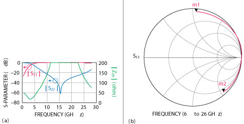
Figure 4 Simulated S-parameters for the shunt detector LPF; S-parameter amplitude and Zin magnitude (a), phase of S11 related to Zin (b).
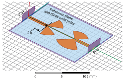
Figure 5 Microstrip realization of an LPF for the series detector.
Design Procedure
Circuit Configuration
Although the application may vary, a conventional detector usually consists of an input matching network, a core detection unit (e.g. diode or FET) and an output lowpass filter (see Figure 1). The output of a demodulation detector is different from a power detector because it is not DC, but is a baseband signal that is passed by a DC blocking capacitor.
Matching to achieve a wide RF operating band is difficult. To address this problem, the conventional input matching network is replaced with an ICN. The ICN provides a flat wide band response and an impedance at baseband frequencies that enables high data rates.
The diode provides nonlinearity to generate new frequency components, including DC and higher order harmonics, or the baseband component for an ASK signal input.1 There are two circuit configurations, i.e. shunt and series (see Figure 2). Both are built and tested to illustrate the effect of the LPF’s input impedance on IF bandwidth and to compare overall performance. The first function of the LPF is to select the desired IF signal generated by the diode and keep the RF frequency and higher order harmonics from reaching the output port.7 The second function is to concentrate RF energy on the diode in order to more efficiently utilize its nonlinearity.
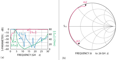
Figure 6 Simulated S-parameters for the series detector LPF; S-parameter amplitude and Zin magnitude (a), phase of S11 related to Zin (b).
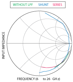
Figure 7 Diode input impedance for different configurations.
Low Pass Filter Analysis and Design
The LPF has a passband and stopband, the passband is matched to a reference impedance (usually 50 Ω), and the stopband is, ideally, either open or short (this is true for any filter). The LPF in Figure 2a, for example, approaches an open circuit in its stopband, so S11 on the Smith Chart is very close to the right, whereas S11 for the LPF in Figure 2b approaches a short on the opposite side. LPFs that simply produce wide stopbands, without considering input impedance, are inadequate for this detector design, because RF energy concentration is dependent upon the LPF’s input impedance in the stopband. This is seldom discussed in the literature.8-10
For the shunt detector, it can be deduced that if the input impedance of the LPF is larger than that of the diode, more RF energy is added to the diode, therefore, the LPF should present a high input impedance in the stopband. Conversely, a low impedance in the stopband will cause a decrease in RF energy added to the diode and hence a decreased working bandwidth. Consider the input impedance of the third-order lumped LPF in Figure 2a:

where ω is the angular frequency and it is assumed to be in the stopband, such that jωL and jωC both have very large values. Thus, Zin1 is an inductive high impedance, which features an open stopband property and satisfies the requirement discussed above. In microstrip, a high impedance line (narrow width) is used to realize a series inductor (see Figure 3).
In practice, it is difficult to maintain a high Zin for the microstrip LPF in Figure 3 over a wide stopband. This may be addressed by restricting the length or the order of the filter. Although high order (implying large size and length) provides excellent suppression, it also introduces parasitics so that a high impedance line or radial stub cannot be simply treated as a series inductor or shunt capacitor, respectively, and the property of Zin changes with frequency. Examples of LPF designs in the literature8-10 have frequency dependent stopband properties, i.e. S11 phase moves from one side of the Smith Chart to another. To reach an acceptable compromise between bandwidth and suppression, no higher than third-order is chosen.
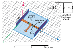
Figure 8 ICN for the shunt detector along with simplified equivalent circuit.
Figure 4 shows the simulated results of the shunt LPF. Port 1 is shifted to the reference plane where Zin is calculated. Figure 4b shows that S11 falls on the right side of the Smith Chart, which means the magnitude of its input impedance|Zin| is larger than 50 Ω. The closer it is to the right endpoint, the larger the impedance. |S21|, which is better than -10 dB from 6 to 26 GHz, shows that good suppression is simultaneously achieved.
For the series detector, the input impedance must be low to ensure that RF energy is concentrated on the diode. Consider the third-order lumped filter shown in Figure 2b:

where ω is also assumed to be in stopband. Thus Zin2 is a capacitive low impedance, which features low impedance stopband properties. In microstrip, a shunt radial stub is used to realize a shunt capacitor (see Figure 5). Figure 6 shows the simulation results for the series LPF. S11 is on the left side of the Smith Chart, which means |Zin| is smaller than 50 Ω. |S21| is better than -15 dB from 6 to 26 GHz.
Although suppression of 10 or 15 dB is not as good some LPFs with wide and deep suppression bands,8-10 they do not consider the input impedance or phase of S11. It is necessary to consider not only suppression but also input impedance in the stopband when designing a wideband detector or other wideband devices like mixers. The two LPFs described in this article have input impedances that focus more RF energy on the diode and utilize its nonlinearity more efficiently, resulting in higher sensitivity and wider working bands.
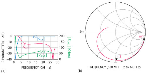
Figure 9 Simulated S-parameters for the shunt detector ICN; S-parameter amplitude and Zout magnitude (a), phase of S22 related to Zout (b).

Figure 10 ICN for the series detector along with simplified equivalent circuit.
Impedance Conversion Network Design
Conventionally, the diode’s input impedance is often matched to 50 Ω over a narrow RF frequency band in order to obtain a high output voltage. As shown in Figure 7, this is because the input impedance of the diode at different frequencies is dispersed across the Smith Chart far away from the center, making wideband matching difficult to achieve. In this design, sensitivity is traded for flatness, by replacing the matching network with an ICN. In order to demodulate a high bit rate ASK signal, the ICN must convert 50 Ω to an appropriate impedance as seen from the diode to the network at baseband frequencies.
A high impedance must be presented at baseband frequencies to the shunt type detector. As shown in Figure 8, a simplified baseband equivalent circuit (ignoring reactive elements) is a current source with two parallel resistors, one representing the output load (RL) and the other representing the magnitude of the input impedance looking into the ICN (|Zout|). The larger |Zout| relative to RL, the more baseband energy is transmitted to the load.
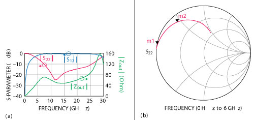
Figure 11 Simulated S-parameters for the series detector ICN; S-parameter amplitude and Zout magnitude (a), phase of S22 related to Zout (b).
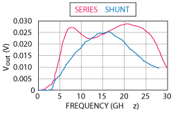
Figure 12 Simulated detector output (Excitation: –5 dBm; load: 50 Ω).
A three order half lumped element microstrip highpass filter (HPF) is designed to realize the ICN for the shunt type detector. ‘Half lumped’ means that the HPF is composed of both distributed and lumped elements. The lumped elements are two single layer capacitors, because it is difficult to attain enough capacitance using distributed techniques.
The simulated results (an HPF response) are shown in Figure 9. Figure 9b shows that the magnitude of the output impedance is converted from 50 Ω (source impedance) to a larger value in the baseband (e.g. 80 Ω at 2 GHz). In the RF band, the output impedance is around 50 Ω, which does not match the diode input impedance (generally not 50 Ω). This mismatching method is frequently used in wideband design, because there is always a trade-off between match and bandwidth. An additional attenuator may be introduced between the source and detector to reduce the effect of unmatched energy on source.
For the series detector, in which diode bridges over the ICN and LPF, a low impedance must be presented in the baseband. A simplified baseband equivalent circuit (see Figure 10) is a voltage source cascaded with |Zout| and RL. The smaller |Zout| is relative to RL, the more baseband energy is transmitted to the load.
The ICN for the series type detector consists of three sections of stepped impedance transmission line and a high RF impedance shorted stub in parallel at the end of the second section. The stub provides a DC path for the series diode and low impedance at baseband.
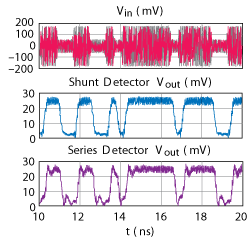
Figure 13 Simulated demodulation wave- form (2.5 Gbps).
The simulation results are shown in Figure 11. This ICN converts the magnitude of the output impedance from 50 Ω(source impedance) to a smaller value in baseband (e.g. 24 Ω at 2.5 GHz). In the RF band, the three sections of stepped impedance are optimized for a flat response of baseband output with the aid of EDA tools.
Total Circuit Simulation
The simulated DC output of the two detectors is shown in Figure 12. RF excitation is -5 dBm from 0.1 to 28 GHz, and the load termination is 50 Ω. Total fluctuation F and narrow band fluctuation F' within 1 GHz are defined as follows:

For the shunt detector, in the working band of 6 to 26 GHz, the maximum and minimum outputs are 25 and 8 mV, so that F = 4.9 dB. The worst F'(x) = 1.094 dB when x = 7 GHz. For the series detector, F = 1.061 dB appears between outputs of 28 and 22 mV. The worst F'(x) = 0.7 dB when x = 7 GHz.
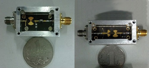
Figure 14 Fabricated detectors; shunt (a), series (b).
As a rule of thumb, a pseudo random binary sequence (PRBS) digital signal with bit rate of x Gbps covers x GHz spectrum. The passband of the LPF is designed to be 4 GHz, so the two detectors can work up to a 2.5 Gbps baseband signal rate. A simulated demodulation waveform is shown in Figure 13, in which the carrier frequency is 16 GHz.

Figure 15 Simulated versus measured open circuit output voltage; shunt detector (a), series detector (b).
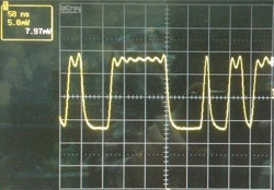
Figure 16 Measured demodulation wave- form (50 Mbps).
Measured Results
The fabricated detectors are shown in Figure 14. The DC output voltages and the baseband demodulation waveforms are measured. For the DC measurements, output voltage measured with a high impedance voltmeter is proportional to the output with 50 Ω, and is more convenient to measure. Simulation with a 10 MΩ termination is compared with the measured results. The input RF power is -5 dBm. Output voltage under this condition is the open circuit output voltage. Comparisons are shown in Figure 15.
Measured and simulated results agree closely in the 6 to 26 GHz band, verifying the design ideology and procedure. Small deviations are due to standing waves caused by mismatch, manufacturing inaccuracies or imperfections in the diode model. For the shunt detector, the open circuit output voltage varies from 25 to 82 mV, with a total fluctuation of 5.31 dB. The worst-case narrowband fluctuation is 1.59 dB. For the series detector, the open circuit output voltage varies from 68 to 146 mV, with a total fluctuation of 3.32 dB. The worst-case narrowband fluctuation is 1.07 dB. The series detector demonstrates better performance than the shunt detector. Both have total fluctuations better than 7.5 dB (reported by Alamri and Alamoudi).6
Figure 16 shows the demodulation waveform of a 50 Mbps ASK PRBS signal with a carrier frequency of 16 GHz, and with a 50 Ω output termination. Table 1 compares the performance of these detectors with other reported results.
Conclusion
Two types of detectors, shunt and series, are designed and fabricated. Measured output voltage responses correspond closely with the simulated results, which demonstrate the feasibility of the design procedure. The minimum open circuit output voltages of the two detectors are measured to be 25 and 68 mV, respectively, with -5 dBm input RF power. Narrowband fluctuation is less than 1.59 dB for the shunt detector and is less than 1.07 dB for the series detector. The average output voltage of the series type is higher than that of the shunt type.
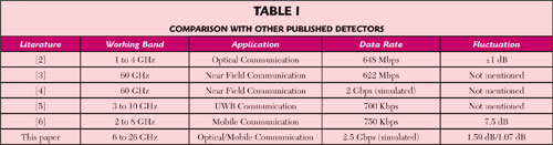
Compared with other published detectors, the prototypes described in this article have very wide operating bands (6 to 26 GHz) and relatively flat frequency responses. Their impedance conversion networks have sufficient bandwidth to demodulate up to a 2.5 Gbps ASK signal. The detectors are suitable for use in many modern communication systems including mobile and coherent optical.
References
- D.M. Pozar, Microwave Engineering, 3rd ed., Wiley, New York, 2005.
- P. Ghiggino, “Novel Square-Law Demodulator for use in Coherent ASK/FSK Heterodyne Optical Receivers,” ElectronicsLetters, Vol. 25, No. 12, June 1987, pp. 803-805.
- M. Ko, H.S. Kang and W.Y. Choi, “A CMOS-Compatible Schottky-Barrier Diode Detector for 60-GHz Amplitude-Shift Keying (ASK) Systems,” IEEE MTT-S International Microwave Symposium Digest, June 2008, pp. 1557-1560.
- H. Zirath and Z. He, “Power Detectors and Envelope Detectors in mHEMT MMIC-Technology for Millimeterwave Applications,” European Microwave Integrated Circuits Conference Digest, September 2010, pp. 353-356.
- S. Sankaran and K.K.O. “An Ultra-Wideband Amplitude Modulation (AM) Detector Using Schottky Barrier Diodes Fabricated in Foundry CMOS Technology,” IEEE Journal of Solid-State Circuits, Vol. 42, No. 5, May 2007, pp. 1058-1064.
- S.M. Alamri and A. Alamoudi, “S-C Bands Broadband Envelope Detector Design,” Saudi International Electronics, Communications and Photonics Conference (SIECPC) Proceedings, April 2011, pp. 1-6.
- D.M. Pozar, Microwave and RF Wireless Systems, Wiley, New York, 2001.
- I.S. Kim and S.W. Yun, “Compact LPF Using Asymmetrical Microstrip Step Discontinuity for Harmonic Suppression,” Electronics Letters, Vol. 41, No. 16, August 2005, pp. 41-42.
- M. Hayati, S. Majidifar and O.S. Fathabadi, “Compact Microstrip Lowpass Filter with Wide Stopband and High Attenuation,” Microwave Journal, Vol. 55, No. 4, April 2012, pp. 90-98.
- Y. Yousefzadeh and M. Hayati, “Compact Lowpass Filter with Wide Stopband Using a Tapered Microstrip Resonator Cell,” Microwave Journal, Vol. 55, No. 3, March 2012, pp. 122-128.