
The need to continually improve power amplifier (PA) efficiency and linearity has resulted in a broad range of evolving technologies that are driving PA test requirements. To address these requirements, this article covers developments in modern cellular handset PA test and evaluation techniques including: digital pre-distortion (DPD) testing, envelope tracking (ET) characterization, and load pull as key parameters to characterize the device.
In order to understand the context of new test requirements, one must first consider that a PA will generally operate with highest efficiency as it nears its saturation region – a region often characterized by highly nonlinear behavior. In addition, high peak-to-average power ratio (PAPR) characteristics of modern communications signals such as LTE or 802.11ac exacerbate this condition by requiring greater back-off to avoid distortion.
Increasingly popular technologies such as DPD, ET and load pull are each designed to improve either the linearity or efficiency of the PA to address these challenges. DPD effectively linearizes a PA at higher output powers and improves the likelihood that the device will meet standard-specific transmission requirements for modulation quality and spectral purity. Envelope tracking is aimed at improving efficiency for high-PAPR waveforms by dynamically changing the efficiency profile of the device. Finally, load pull enables engineers to improve the overall efficiency of the device by finding the optimal input and output impedance of the power transistor.
Testing DPD-Enabled PAs
The combination of increasing signal processing capabilities combined with the use of more challenging signals such as LTE has increased the use of DPD technology in mobile devices. DPD algorithms improve modulation quality and reduce spectral re-growth in the frequency domain – especially at higher output power levels.
In the past, PA characterization required only a vector signal generator (VSG) to produce the modulated signal and a vector signal analyzer (VSA) to measure the output. While powering the PA with a power supply or source measure unit (SMU), one would measure characteristics such as error vector magnitude (EVM) and adjacent channel leakage ratio (ACLR).
Although PA testing has historically required fairly simple instrumentation and measurement practices, testing of today’s DPD-enabled PAs is more complex. Given the increased likelihood that a PA will transmit pre-distorted waveforms in its end use, engineers are less interested in its raw performance and are more interested in its ability to be pre-distorted with one of several common DPD algorithms. As a result, modern PA testing requires engineers to mimic the functionality of the DPD algorithm with advanced test equipment.
Approaches to DPD
Two DPD implementations that are gaining increasing interest are the simple memoryless look-up table (LUT) and more complex algorithmic techniques based on the Volterra series. In both implementations, the DPD model is derived from stimulus-response measurements that require one to compare input signals introduced to the PA with the acquired output signals. Although engineers traditionally performed common stimulus-response measurements like AM-AM and AM-PM with a vector network analyzer (VNA), these instruments are traditionally unable to provide modulated signals.
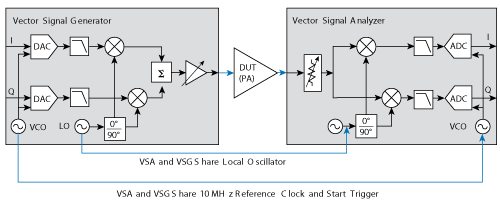
Figure 1 Block diagram of a VST-based PA measurement system.
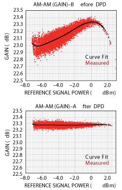
Figure 2 DPD algorithms correct the AM-AM response of the PA.
An increasingly popular method to measure AM-AM and AM-PM is with a modulated stimulus that is generated with a VSG and acquired with a VSA. By comparing both the input and output power and phase on a sample-by-sample basis, one can measure AM-AM and AM-PM. Not only does the VSG-VSA approach capture the memory effects of the PA, but it also enables the use of more sophisticated DPD models.1
Measuring AM-AM and AM-PM
When measuring AM-AM and AM-PM using a VSG and VSA, it is extremely important to share any and all clock signals to avoid measurement error. Note that although VNAs inherently share timing signals between stimulus and response, VSAs and VSGs historically do not. As shown in Figure 1, important timing signals including the local oscillator (LO) and the 10 MHz reference clocks can be easily shared on an NI vector signal transceiver (VST). Note that LO sharing is generally only possible in direct conversion VSAs and VSGs. In more traditional IF-based VSAs, the LO frequency will inherently offset the center frequency of the signal being acquired. Thus, when using an IF-based VSA, LO synchronization is not possible and sharing a 10 MHz reference clock is the best alternative.
The memoryless LUT approach to DPD uses measured AM-AM and AM-PM data to construct a simple LUT. Based on the measured data, the LUT predicts the needed power and phase of each input sample in order to achieve a linear output response. As observed in Figure 2, the AM-AM response of a memoryless LUT-corrected PA achieves almost constant gain versus output power. The resulting signal is characterized by reduced spectral re-growth in the frequency domain.
One can also see the relationship between the “measured” response and the “curve fit.” Especially with wideband signals, PA memory effects create a scenario where the phase and magnitude of the output signal cannot be completely predicted by the phase and magnitude of the input signal. Thus, even though measuring AM-AM and AM-PM with a VSG and VSA captures memory effects, the memoryless LUT model does not compensate for memory effects directly.
Volterra Series and Memory Polynomial Model
A more comprehensive model for nonlinear systems with memory is a Volterra series2 (see Equation 1). The Volterra series can be computationally intensive, and the complexity of this model increases drastically with increasing nonlinearity order (K) and memory depth (M).
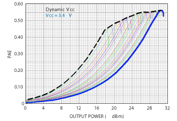
Figure 3 PAE vs. power out across Vcc.
In practice, nonlinear systems with memory can be adequately modeled with only a subset of the terms in a full Volterra series. Common models based on this approach include the memory polynomial, the Weiner, and the Hammerstein models.3 Because these models are considerably simpler to implement, they are more practical for modern mobile devices.
Similarly to the memoryless LUT, testing of DPD-enabled PAs that use models based on a Volterra series requires a modulated stimulus and response. In general, it is desired that the instrumentation supports signal bandwidths three to five times the bandwidth of the waveform. In addition, many test equipment vendors provide software to control both the VSG and VSA and implement the model within the instrumentation itself. These software utilities enable the engineer to characterize the ability of the PA to be pre-distorted (based on the predictability of its distortion) without requiring an intimate knowledge of the model.
Envelope Tracking
A second increasingly important test requirement for wireless PAs is the ability to test under envelope tracking conditions. Envelope tracking technology is based on two fundamental premises:
- Modulated signals have an inherently non-zero PAPR
- PA efficiency increases as the device approaches saturation
Given these premises, one can improve overall PA efficiency by operating the device close to its saturation point as often as possible.
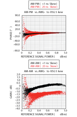
Figure 4 AM-PM and AM-AM distortion with < 1 ns and 20 ns of skew.
Because modern communications signals tend to have relatively high PAPRs (LTE uplink is 6 to 8 dB), one straightforward method to improve overall PA efficiency is to modulate the Vcc signal such that it tracks the envelope of the RF signal.4,5 By effectively modulating the Vcc signal in real-time, it is possible to better optimize instantaneous output power over a range of output power levels. As shown in Figure 3, power-added efficiency (PAE) is actually a function of output power and Vcc. Thus, one can optimize PAE by instantaneously choosing the lowest Vcc necessary to achieve the desired output power.
It is worth noting that the process of modulating Vcc as a function of desired output power creates two specific requirements on the system. First, because PA gain is also a function of Vcc, merely modulating the Vcc signal introduces AM-AM distortion that must be corrected with DPD algorithms. Second, modulating the Vcc signal introduces additional synchronization requirements between instruments sourcing the RF input and the modulated Vcc signal.
Synchronization in ET Testing
A typical envelope tracking test system includes an RF signal generator to provide RF input to the PA and an arbitrary waveform generator (AWG) to provide the shaped Vcc signal. In this test system, both instruments must be tightly synchronized. The synchronization requirements of an ET PA test bench are fairly significant. In practice, the method by which an ET PA achieves higher PAE is to associate each input power level with a corresponding Vcc control voltage. Moreover, because PA gain is a function of Vcc, skew or jitter between the Vcc and RF input signals can introduce significant additional AM-AM and AM-PM distortion.
If, for example, the Vcc waveform lags the RF signal, the power modulator will not supply ample power to the device at the peak output power of the input waveform. A similar situation occurs if Vcc leads the RF. For wideband signals, even a small amount of skew (more than 10 ns) can significantly affect the performance of the PA.
Sharing Reference Clocks and Start Triggers
One of the most common methods to synchronize the VSG and AWG is through shared reference clocks and start triggers. With both instruments synchronized, one must typically apply a small delay between the VSG and the AWG to compensate for differences in signal path.
Although both skew and timing jitter (variable skew) between the AWG and VSG can impair test results – jitter is the least predictable and is by far the most problematic. Generally, the effects of static skew can be measured either directly as a time domain signal or indirectly through the AM-AM distortion or spectral re-growth it produces. Jitter, however, is much more difficult to compensate for as it is frequently the result of the instrumentation architecture. Note that PXI instruments are generally subject to less AWG-to-VSG jitter due to PXI’s use of an internal 10 MHz system clock that provides all modules with a timing reference that offers < 1 ns channel-to-channel skew.6
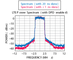
Figure 5 Spectral regrowth with < 1 ns and 20 ns of skew
The effect of AWG-to-VSG skew on AM-AM and AM-PM distortion can be observed in Figure 4. With < 1 ns of skew, curve fitting the gain versus output power is relatively straightforward – as there is very little deviation. However, with 20 ns of skew between the AWG and VSG, there is significant AM-AM distortion and lower gain. Not only does this distortion create spectral re-growth, but the wider “spread” of the AM-AM and AM-PM makes pre-distortion more difficult.
In the frequency domain, one can easily observe the effects of AM-AM distortion introduced by poor synchronization between the AWG and VSG. Figure 5 shows the resulting signal in the frequency domain with a memory polynomial DPD algorithm applied. The configuration with 20 ns of skew provides worse ACLR performance. Given this result, one common technique to identify VSG-to-AWG misalignment is to measure ACLR as a function of skew. Because skew ultimately results in worse ACLR, the optimal AWG-to-VSG delay can be identified by choosing the best-case ACLR as a function of programmatic delay.
Load Pull
The third PA optimization technique is load pull. Although engineers have been using load pull test systems for many years to test extremely high power PAs for wireless infrastructure equipment – increasing efficiency demands of handset PAs has made load pull measurements more pervasive over a wider range of modern PAs.
The basic approach is to experimentally identify the ideal source and load impedance of a PA to achieve the highest possible PA efficiency. By identifying these ideal impedances, a PA designer can then develop corresponding impedance matching networks.7
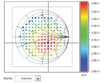
Figure 6 Load pull plots on Smith Chart.
A traditional source and load pull setup presents a wide range of source and load impedances to the PA under varying RF input power and DC bias conditions.8,9 By measuring PA output power as function of source and load impedance, one can identify the impedances that will produce the highest output power. Moreover, by measuring DC bias voltages and currents as well, one can also measure output efficiency and power added efficiency (PAE) as a function of impedance. The results are typically visualized as contour plots on a Smith Chart (see Figure 6), or imported into EDA tools such as the AWR design environment.
Source and Load Pull Challenges
Traditional source and load pull measurement systems use power meters to measure input and output powers under CW conditions. Unfortunately, due to their measurement principle and wideband nature, power meters are typically slow and cannot resolve power between the fundamental frequency and harmonics.
Modern load pull measurement systems10 typically use vector instrumentation such as a VNA, a large signal network analyzer (LSNA), a VSG used in conjunction with a VSA, or a broadband oscilloscope (see Figure 7). These types of instruments offer inherently faster, frequency-selective, measurements – although only systems using a VSG offer a modulated stimulus. For example, a PXI-based load pull system11 with an NI vector signal transceiver and Maury impedance tuners includes both a VSG and a VSA to support both CW and modulated stimulus of the DUT.
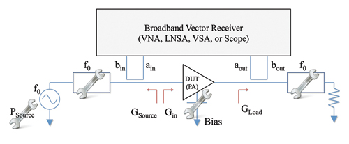
Figure 7 Modern source and load pull setup.
Note that the impedance presented to the PA can be formalized as a complex value (real and imaginary part or amplitude and phase) in different formats: impedance (Z), voltage standing wave ratio (VSWR), or reflection coefficient (Γ), i.e. the ratio between incident and reflected travelling waves, with respect to the observed impedance. In fact, source and load pull systems can introduce various impedances to a PA either by adjusting the impedance directly (passive tuning), or by emulating a particular impedance by actively injecting a signal (active tuning).
Passive Tuning
Traditional source and load pull measurement systems use passive mechanical tuners to affect the impedance conditions of a circuit. In this scenario, the tuner presents various impedances to the PA by perturbing the electric field of an airline using a metallic probe (called a “tuning slug”). By selecting the appropriate vertical and horizontal positions of the probe with respect to the airline, a mechanical tuner can be configured to provide a wide range of impedance conditions. Generally, passive mechanical tuners change impedance relatively slowly compared to other tuning systems because they require moving mechanical parts.
Recently, new approaches to passive tuning include passive electronic impedance tuners based on PIN diodes or MEMS technology. Such tuners overcome the speed issue of traditional passive mechanical tuners by electronically changing the length of stubs along a transmission line. However, these tuners can typically present only a limited set of impedances on the Smith Chart compared to passive mechanical tuners.
Unfortunately, passive tuning systems have significant drawbacks when testing PAs designed for wideband communications signals such as LTE. Because the impedance of a device can vary over the modulation bandwidth, performing load pull measurements with a modulated stimulus provides a more accurate representation of how the PA will perform under particular impedance conditions.
Active Tuning
Active tuning systems can be further grouped into two sub-categories: open-loop and closed-loop architectures. Unlike passive tuning, which involves the manual creation of a specific impedance, the principle of active tuning is to create the desired impedance condition by injecting additional signals into the PA.
Closed-loop active tuning systems use a part of the incident wave, through a coupler or a circulator, to emulate the desired impedance condition. In this setup, a combination of variable amplifiers and phase shifters modify the incident wave, both in amplitude and phase, before sending it back to the DUT as the reflected wave. Because the synthesized reflection is electronically controlled, the tuning process can be quite fast. Although the synthesized reflection is fully synchronous with the incident wave even when the incident power changes, closed-loop active tuning systems are subject to oscillation depending on their architectures.
Recently, NI demonstrated a PXI-based pseudo closed-loop active tuning system developed in cooperation with Mesuro.12 This system samples the incident signal with the help of a downconverter and passes it to an onboard FPGA. Inside the FPGA, the phase and amplitude of the sampled incident signal are digitally controlled before generating the reflection with an RF signal generator.
In addition to closed-loop active tuning systems, one can adjust the effective output impedance of a DUT using an open-loop approach. Open-loop active tuning systems use external RF sources to generate and control the amplitude and phase of the reflected wave. Although these systems avoid the oscillation issues present in closed-loop systems they require tight synchronization between each of the signal generators.
In this context, a new mixed-signal open-loop active load pull system has been patented by Anteverta Microwave and developed in cooperation with NI. Using external frequency upconverters and downconverters, the Anteverta system benefits from tightly synchronized PXI arbitrary waveform generators and analog-to-digital converters (ADC) to generate and capture wideband modulated signals at baseband.13
Conclusion
With the emergence of more sophisticated PA technologies, testing today’s handset PAs is becoming more complex. As a result, engineers must understand how to characterize PAs designed to operate under DPD and ET conditions and even construct more sophisticated load pull test systems. Fortunately, each of these measurement conditions is reasonably straightforward and can be addressed through modern test instrumentation.
References
- F.M. Ghannouchi and O. Hammi. “Behavioral Modeling and Predistortion,” IEEE Microwave Magazine, Vol. 10, No. 7, December 2009, pp. 52-64.
- D.R. Morgan, Z. Ma, J. Kim, M.G. Zierdt and J. Pastalan. “A Generalized Memory Polynomial Model for Digital Predistortion of RF Power Amplifiers,” IEEE Transactions on Signal Processing, Vol. 54, No. 10, October 2006, pp. 3852–3860.
- L. Ding, G.T. Zhou, D.R. Morgan, Z. Ma, J.S. Kenney, J. Kim and C.R. Giardina, “A Robust Digital Baseband Predistorter Constructed Using Memory Polynomials,” IEEE Transactions on Communications, Vol. 52, No. 1, January 2004, pp. 159-165.
- D. Kim, J. Choi, D. Kang and B. Kim, “High Efficiency and Wideband Envelope Tracking Power Amplifier With Sweet Spot Tracking,” IEEE Radio Frequency Integrated Circuits Symposium, May 2010, pp. 255-258.
- M. Hassan, Myoungbo Kwak, V.W. Leung, C. Hsia, J.J. Yan, D.F. Kimball, L.E. Larson and P.M. Asbeck, “High Efficiency Envelope Tracking Power Amplifier With Very Low Quiescent Power for 20 MHz LTE,” IEEE Radio Frequency Integrated Circuits Symposium, June 2011, pp. 1-4.
- National Instruments NI-TClk Technology for Timing and Synchronization of Modular Instruments, www.ni.com/white-paper/3675/en/
- S.C. Cripps, RF Power Amplifiers for Wireless Communications, Second Edition, Artech House, 2002, ISBN 978-1596930186.
- Application Note 5C-029, “Measurement of Large-Signal Device Input Impedance during Load Pull,” Maury Microwave Corp.
- Application Note 08, “Basics on Load Pull and Noise Measurements,” Focus Microwaves.
- Application Note 5A-051, “Vector-Receiver Load Pull Measurement,” Maury Microwave Corp.
- “Load-Pull LabVIEW Example Combining NI VST or NI VSG/VSA and Maury Microwave LXI Tuner,” National Instruments Corp, https://decibel.ni.com/content/groups/network-analysis.
- “Mesuro Launches Rapid Load Pull Test Solution,” Press Release, Microwave Journal, www.microwavejournal.com/articles/19999.
- M. Marchetti, M.J. Pelk, K. Buisman, W. Neo, M. Spirito and L.C.N. de Vreede, “Active Harmonic Load-Pull With Realistic Wideband Communications Signals,” IEEE Transactions on Microwave Theory & Techniques, Vol. 56, No. 12, December 2008, pp. 2979-2988.