
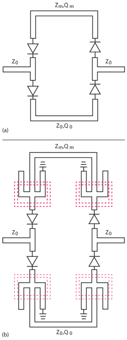
Figure 1 Conventional (a) and proposed phase shifter (b).
This tunable dual-band phase shifter uses a defected ground structure (DGS) and stubs. Its frequency can be tuned by changing the length and width of the stubs and the dimensions of the DGS. The resulting circuit has improved insertion loss and return loss with reduced phase variation, as verified by measurement.
hase shifters are essential components in transmit/receive phase array antenna elements. While there are well known transmission line phase shifter approaches with sufficient performance, such as all-pass filter (APF) networks and vector addition,1,2 they generally lack tunability. MEMS and varactor-tuned substrate integrated waveguide (SIW) are used to achieve tunable performance; however, these methods introduce increased design complexity.3,4 The composite right-/left-handed transmission line (CRLH-TL) structure is also used,5,6 with the penalties of increased physical size and insertion loss.
Providing advantages such as circuit size reduction and spurious response suppression, the DGS has been used successfully in the design of microwave circuits, such as filters, power dividers, couplers, amplifiers and oscillators.7,8 Modern communication systems require dual-band bandpass filters (BPF) with low insertion loss, high selectivity and compact size, driving an increased interest in dual-band filters employing the DGS structure.9,10
This article describes the design of a 6 bit digital phase shifter using a DGS in the form of a rectangular ring and incorporating open and short-circuited stubs to create a tunable dual-band phase shifter. The length and width of the stubs (upper layer) and the dimensions of the rectangular ring (bottom layer) are adjusted to achieve the desired center frequencies and bandwidths.
Analysis
The configurations of the conventional and proposed structure are shown in Figure 1. The proposed structure includes two layers. In the upper layer are two equal length parallel stubs: one open and the other short-circuited. In order to improve its operational bandwidth, the device employs impedance transformers at its input and output ports. When these matching circuits are ignored, the reflection coefficient (Γ) and the transmission coefficient (T) across the plane are by given by11
where b is the normalized susceptance of the stubs connected in parallel with the main microstrip line given by
where θs and Zs are the electrical length and impedance of the stubs at the design frequency f0. Measured against the reference microstrip line, the differential phase shift is given by
where θr is the electrical length of the reference microstrip line at frequency f0.
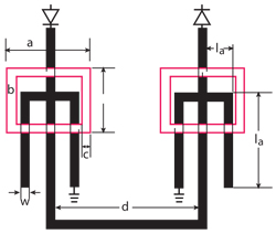
Figure 2 Schematic of the DGS rectangular ring and tuning stubs.
Design
The schematic of the rectangle ring DGS and stubs is shown in Figure 2. The upper resonator is implemented using open and shorted stubs and the lower resonator is a DGS in the shape of a rectangular ring. The upper and lower metals are separated by the substrate. The interaction that takes place between the stubs and the DGS is not conventional, so the classical design approach cannot be applied here.
The length and width of the DGS and stubs are a, b, l and w, respectively (l is the sum of la and lb, where la is 1.5 mm). In addition, the width of the slot between the outer rectangle and inner rectangle is c, while the distance between two rectangular rings is d. The frequency can be tuned by adjusting the length and width of the DGS and stubs. The circuit is designed for Rogers 5880 substrate material. Electromagnetic simulation software (HFSS) is used to determine the physical dimensions. With a, b, c and d at 15, 5, 2 and 20 mm, respectively, the simulated |S21| with several different stub lengths and widths is shown in Figures 3 and 4. This shows the narrowing and shifting of the passbands lower in frequency with decreasing stub length and width.
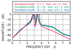
Figure 3 Simulated | S21 | for different stub lengths.
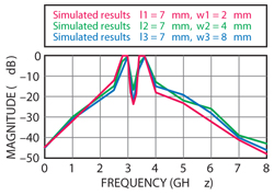
Figure 4 Simulated | S21 | for different stub widths.
Fabrication and Measured Response
The circuit is fabricated on Rogers 5880 substrate material using the Microsemi LSP 1000 PIN diode as the phase switching device. Simulated and measured values of |S21| for the 45° phase shifter bit are shown in Figure 5 for the DGS dimensions a, b, c and d equal to 15, 5, 2 and 20 mm, respectively. The effect of different lengths and widths of the DGS rectangular ring are shown in Figure 6.
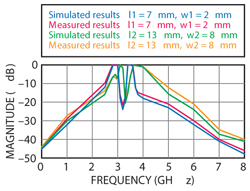
Figure 5 Simulated and measured | S21 | for different stub lengths and widths.
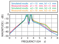
Figure 6 Simulated and measured | S21 | for different DGS lengths and widths.
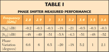
The measured insertion loss, return loss and phase variation for a 6 bit digital phase shifter are shown in Table 1. The insertion loss varies from 0.3 to 0.5 dB and the return loss varies from 48 to 52 dB within the passbands, while the phase variation is controllable to within ±3 degrees. A photograph of the fabricated 6 bit digital phase shifter is shown in Figure 7.
Conclusion
A tunable 6 bit digital phase shifter employing open and shorted stubs and a DGS rectangular ring achieves tunable dual-band performance by adjusting the length and width of the DGS and stubs. The result is improved insertion loss and return loss with reduced phase variation, as verified by measurement.
References
- A.C. Ulusoy, B. Schleicher and H. Schumacher, “A Tunable Differential All-Pass Filter for UWB True Time Delay and Phase Shift Applications,” IEEE Transactions on Microwave Theory and Techniques, Vol. 50, No. 8, August 2002, pp. 1885-1889. G.S.K. Yong and C.E. Saavedra, “A Fully Integated S-Band Vector Phase Shifter in CMOS Technology,” IEEE Topical Meeting Silicon on Monolithic Circuits in RF Systems, January 2009, pp. 1-4.
- C. Fritzsch, F. Giacomozzi, O.H. Karabey, F. Goelden, A. Moessinger, S. Bildik, S. Colpo and R. Jakoby, “Continuously Tunable W-Band Phase Shifter Based on Liquid Crystals and MEMS Technology,” Proceedings of the 41st European Microwave Conference, October 2011, pp. 1083-1086.
- Y. Ding and K. Wu, “Varactor-Tuned Substrate Integrated Waveguide Phase Shifter,” IEEE MTT-S International Microwave Symposium Digest, June 2011, pp. 1-4.
- N. Michishita, H. Kitahara, Y. Yamada and K. Cho, “Tunable Phase Shifter Using Composite Right/Left-Hand Transmission Line With Mechanically Variable MIM Capacitors,” IEEE Antenna and Wireless Propagation Letters, October 2011, pp. 1579-1581.
- J. Zhang, S.W. Cheung and T.I. Yuk, “Design of N-Bit Digital Phase Shifter Using Single CRLH TL Unit Cell,” Electronics Letters, Vol. 46, No. 7, April 2010, pp. 67-68.
- J.S. Lim, C.S. Kim, D. Ahn, Y.C. Jeong and S. Nam, “Design of Low-Pass Filters Using Defected Ground Structure,” IEEE Transactions on Microwave Theory and Techniques, Vol. 53, No. 8, August 2005, pp. 2539-2545.
- S.W. Ting, K.W. Tam and R.P. Martins, “Miniaturized Microstrip Lowpass Filter With Wide Stopband Using Double Equilateral U-Shaped Defected Ground Structure,” IEEE Microwave and Wireless Components Letters, Vol. 16, No. 5, May 2006, pp. 240-242.
- G. Chaudhary, H. Choi, Y. Jeong, J. Lim, D. Kim and J.C. Kim, “Design of Dual-Band Bandpass Filter Using DGS With Controllable Second Passband,” IEEE Microwave and WirelessComponents Letters, Vol. 21, No. 11, November 2011, pp. 589-591.
- E. Corrales, O. Menendez and P. de Paco, “Compact Dual-Band Filter Based on Microstrip-DGS Resonator Pairs,” Proceedings of the 41st European Microwave Conference, October 2011, pp. 464-467.
- Y. Wang and M.E. Bialkowski, “UWB Phase Shifter with Parallel Stubs Terminated with Virtual Short and Ground Slots,” Proceedings of the 40th European Microwave Conference, September 2010, pp. 1166-1169.
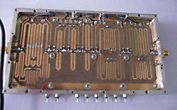
Figure 7 Photograph of the phase shifter employing tuning stubs and DGS.