
New Types of Microstrip Antennas for the Applications
Typically, patch antennas are narrowband and their Q factor is inversely proportional to frequency. The main reason for the high Q factor is that patch antennas are essentially circuits printed on a relatively thin substrate: the higher the dielectric, the higher the Q factor. Over the years, a number of techniques have been developed to increase the patch bandwidth, including adding parasitic and coupling elements. In the context of commercial antennas, these methods can increase the price of the product significantly, simply because the number of parts is doubled and sometimes tripled. Furthermore, the use of dielectric substrates affects not only the cost of these antennas, but their electrical performance as well. This article describes a new type of microstrip patch antenna for UHF frequencies with specific characteristics for use in the wireless communication industry.
Naftali Herscovici
Cushcraft Corp.
Manchester, NH
The expected bandwidth of a printed antenna as a function of frequency, and dielectric constant er and thickness h is shown in Figure 1 . The typical rectangular microstrip patch antenna is extremely narrowband below 1 GHz and, even when printed on a dielectric substrate with a relative permittivity of 2.32, four percent bandwidth (SWR < 2) is the most that can be expected. In this article, a new type of microstrip array is proposed, consisting of a circuit board that includes only the metallized portion of the printed circuit suspended over the ground plane. In the past, some work was performed with suspended microstrip small planar arrays,  usually supported by foam. However, the technique described in this article deals with a new class of microstrip antennas that open new design and application possibilities. This new approach presents a number of advantages over the classical printed microstrip arrays, as well as other types of planar suspended microstrip configurations. The approach also allows the use of three-dimensional transitions, from one level to another, so that the width of the feeding lines can be controlled by changing the spacing between the line and the ground plane. These three-dimensional transitions impact the feed network radiation, radiating elements and coupling between the feed network. In addition, the feeding circuit is purely transverse electromagnetic (TEM), eliminating dispersion and surface waves. This characteristic has a significant impact on the intermodulation characteristics of these types of antennas. The new antenna also supports greater changes in temperature since there is no dielectric substrate (with a temperature expansion coefficient different from that of the metallization). The efficiency is considerably higher since there are no dielectric or surface wave losses. In the case of scanning arrays, the surface wave is removed eliminating the main source for blindness. In some cases, the fabrication cost is considerably lower than that of the conventional type of microstrip antenna since the dielectric substrate is absent. In addition, the new antenna can handle significantly higher power levels (especially CW) and allows for matching techniques similar to those used in waveguide technologies. In this article, two types of microstrip patch antennas for the UHF band are proposed. Based on this technology,2 the antenna types combine new techniques to increase the bandwidth and isolation between ports (for the dual-polarized version).
The Butterfly Patch Fed By a Three-dimensional Feeding Network
The first patch was developed for the wireless Global System for Mobile communications (GSM) band (880 to 960 MHz). To achieve a larger bandwidth, the free  variables for a typical rectangular patch antenna are height and the feeding method. As for the dielectric substrate, it is obvious that using air, more bandwidth, higher efficiency and a lower fabrication cost can be expected. Also, the target was to obtain the required bandwidth using only one element. The basic analysis was performed using the IE3D simulator software package. It was soon realized that in order to obtain the nine percent bandwidth, aside from the height factor, additional methods had to be used. A combination of methods3,4 leads to the butterfly geometry, shown in Figure 2 . The modeling of this antenna showed a high input impedance (approximately 300 W) if fed from the edge. A 135 W point was found 1.2" from the center. A three-dimensional microstrip line consisting of a rectangular transition was used to feed the butterfly patch. Its characteristic impedance changes with height: At 1.3" the characteristic
 impedance is 135 W and at 250 mil it is 50 W (the impedance calculations include the thickness of the metallization, 20 mil). Although this design was completed for UHF, a variety of antennas for
 wireless communication have been developed to cover the other bands, including personal communications service (PCS); personal communications network (PCN); low industrial, scientific and medical (ISM); and high ISM. As the bandwidth of microstrip antennas increases naturally with frequency, larger bandwidths were obtained at higher frequencies, as listed in Table 1. The SWR and radiation patterns of the GSM butterfly antenna are shown in Figures 3 and 4 , respectively. The antenna's front-to-back ratio is approximately 12 dB. In the elevation direction, an 11 dB sidelobe is observed. The antenna was placed asymmetrically in the elevation cut on its ground plane to illustrate the effect of the ground plane on the back radiation. At UHF frequencies, the ground plane should be quite large in order to obtain a better front-to-back ratio.
 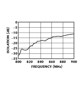 However, these antennas are usually wall mounted so the wall acts (at least partially) as a ground plane, allowing the size of the ground plane to be reduced and effectively determining the size of the antenna. The gain of the antenna is more than 8 dB across the GSM band. A dual-linear-polarized version of this antenna was built and tested, and the isolation between the two ports is shown in Figure 5 . The obtained bandwidth (9.8 percent) in the GSM case is similar to the bandwidth obtained for a traditional stacked patch element (for example, Advanced Mobile Phone Service (AMPS) stacked patch). The stacked patch antenna5 consists of a driven patch and a parasitic patch. The broadband effect is achieved by designing the driven and parasitic patches so they resonate at slightly different frequencies. In some cases, two parasitic elements were used. The cost of the materials used in the stacked-type antennas is almost double that of the materials required to build the butterfly-type antenna. The other butterfly-type antennas are slight modifications of the design described previously, and the best illustration of the achievable bandwidths using this technology is the PCS patch with a 40 percent bandwidth. Again, the main idea in this design is to keep the manufacturing cost as low as possible (use only one patch).
The Waffle Microstrip Patch
The relatively low isolation level obtained in the dual-polarized version of the butterfly antenna leads to a new configuration where the excitation of the cross-polar currents is reduced considerably. Elimination of the cross-polar currents was achieved by utilizing square apertures on the patch, as shown in Figure 6 . Figure 7 shows the isolation of this antenna is significantly better than that of the butterfly dual-polarized patch. Figure 8 shows the radiation patterns of the waffle antenna at 864 MHz. The gain is more than 8 dB across the band. A number of various waffle patches were designed at various UHF bands and the bandwidth obtained was nine to 10 percent, which is the typical bandwidth used in the wireless communication industry.
Figure 6 
Figure 7 
Figure 8
Conclusion
A new technology has been presented for the fabrication of microstrip antennas in general and for UHF frequencies in particular. These antennas are less expensive to construct than the traditional printed patches (they use one patch and no dielectric substrate) and also exhibit good electrical characteristics.
Acknowledgment
The IE3D simulation software is a product of Zeland Software Inc., Fremont, CA
References
1. I.J. Bahl and P. Bhartia, Microstrip Antennas, Artech House, Norwood, MA, 1980.
2. Naftali Herscovici, "New Considerations in the Design of Microstrip Antennas," to be presented at the IEEE Antenna and Propagation Symposium, Montreal, Quebec, Canada, July 1997.
3. Naftali Herscovici, "Suspended Three-dimensional Microstrip Radiators," Patent Application #08/669,047, April 1995.
4. R. Zetner, J. Bartolic and E. Zetner, "Electromagnetically Coupled Butterfly Patch Antenna," Journees Internationales de Nice sur les Antennes, November 12-14, 1996.
5. I.R. James and P.S. Hall, Microstrip Antennas, Peter Peregrinus Ltd., 1989.
Naftali Herscovici received his BSc, MSc and PhD in electrical engineering in 1978, 1985 and 1992, respectively. Between 1983 and 1989, he was employed as an antenna engineer at Rafael, Haifa, Israel, where he was engaged in research and development of microwave antennas. Currently, Herscovici is with Cushcraft Corp., Manchester, NH. His research interests include microstrip arrays, reflector antennas and feeds, pattern synthesis and antenna modeling. He is chairman of the IEEE Antenna and Propagation Society, Boston Chapter.