
Editor’s note: As a part of our ongoing coverage of the evolution of the mobile RF front end, Skyworks has contributed the following piece about how a best-of-breed approach will meet the future needs of this market. Previously, our June cover story, contributed by Qualcomm, described its new all single module CMOS approach to meet the future needs of the mobile RF front end.
Consumer demand for thinner mobile platforms with extended talk times and lightning fast, anytime anywhere data access is driving the need for an unprecedented level of analog and RF complexity for smartphones, tablets and ultrabooks. This is particularly true as the wireless market transitions to 4G and 5G technologies, where the front end architectural challenges have never been greater and are being compounded by the emergence of demanding coexistence, shielding and harmonics issues, not to mention the traditional power efficiency, size and cost constraints.
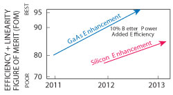
Figure 1 GaAs vs. CMOS enhancements.
As a result, OEMs are increasingly focused on uniquely defining their RF architectures as a means to differentiate their platforms, battling for consumer mindshare and operating system leadership. Consequently, front end circuit board real estate has become precious beachfront property as system providers seek high performance and highly flexible solutions for the next generation flagship platforms. At the same time, as the R&D, IP and manufacturing scale requirements grow to support LTE, W-CDMA and GPRS/EDGE as well as WiFi, GPS, Bluetooth®, Mobile TV, RFID and other non-cellular services, the list of viable suppliers capable of addressing all of these applications is significantly narrowing. The stakes have never been higher and the distinction between winners and losers will undoubtedly become much more apparent over the coming years.
Two Distinct Front end Approaches: Best-Of-Breed versus All Silicon
Over the past decade, leading system-level innovators including Infineon, Ericsson, Freescale, Renesas, Silicon Labs, STMicrolectronics and Texas Instruments, among others, have aggressively pursued the leveraging of silicon processes to address RF front end requirements. Despite the attractiveness of designing in a ubiquitous, bulk silicon process technology, this approach has been met with limited success. Not a single such device is in high volume production and, in virtually all cases, investment has ceased. This is because GaAs performance in the front end has prevailed and continues to push the performance envelope for the foreseeable future (see Figure 1), even with new technologies that improve CMOS performance, such as envelope tracking. By using those same technologies, GaAs maintains its 10 percent plus performance advantage. Further, the performance gap between the two processes across several other metrics including cycle time (see Figure 2), and cost per fabrication mask run is dramatic and certainly not lost on system integrators who strive for time to market advantages, extended battery life and smaller form factors.
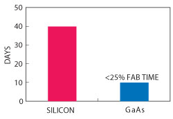
Figure 2 Fabrication cycle time.
The underlying reason for silicon’s limited success as a power amplifier platform is quite simple. When given the choice, OEMs opt for better power added efficiency (PAE) and lower cost as well as faster time to market provided by other process technologies and architectures. CMOS or SOI amplifiers still have a place in the market. It is just not where efficiency and ruggedness are paramount.
Nevertheless, new claims within a system-oriented model have recently emerged and once again, untested arguments for silicon integration and product standardization sound compelling. However, simple physics and the inexorable need for a barrier between the amplifier and the transceiver dictate that the front end will neither be subsumed by the RF section nor will it follow Moore’s law given limited scalability in silicon.
Most importantly, while there is a certain degree of elegance associated with offering a complete, standardized solution to address all of the forthcoming cellular band requirements, a product must still meet OEM expectations across several key metrics including performance, size, cost and time to market. The failure to satisfy all requirements and expectations will not suffice – a design is only as strong as its weakest link.
At a higher level, market demand for the best performing solutions has shown that an integrated silicon approach imposes significant performance trade-offs with limited design flexibility – an unacceptable approach in a performance-driven and fast-moving market. Instead, OEMs prefer to choose their own band configurations and are also quite comfortable mixing and matching components to achieve performance at a competitive cost, while differentiating their products.
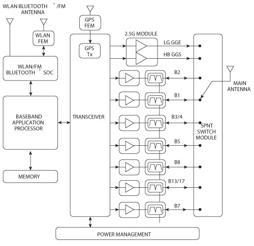
Figure 3 Example of a discrete implementation approach.
Next Generation Solutions

Figure 4 System in a package solution comprised of low band high band 2G/2.5G/3G/4G multimode, multiband power amplifier modules (GaAs), low and high band select switches (SOI) and a controller (CMOS).
With approximately 50 bands either being deployed or soon to be established, OEMs and system engineers alike are searching for architectures to adequately manage the proliferation of bands and the increasing complexity of RF front ends. While the vast majority of OEMs prefer to address the challenge by leveraging best-in-class discrete solutions and system-in-a-package solutions to optimize performance (see Figures 3 and 4), others prefer a completely integrated front end system.
Regardless of the preferred architecture, leading manufacturers like Skyworks have amassed valuable expertise spanning multiple process technologies including CMOS, SiGe, SOI, BiCMOS and GaAs, among others, and has developed an arsenal of advanced and proprietary packaging techniques to deliver the highest performing systems solutions. This capability allows Skyworks to create systems that are specifically tailored to OEM platforms and applications.
SkyOne™, for example, is a platform that integrates all the RF and analog content between the transceiver and antenna. SkyOne leverages Skyworks’ full technology portfolio and advanced multichip module capabilities including proprietary shielding and packaging and is the world’s first semiconductor device to condense multiband power amplifiers and high throw switches along with all associated filtering, duplexing and control functionality into a single, ultra-compact package, all in less than half the area of the industry’s most advanced approach. At the same time, this solution provides the best linearity and power added efficiency for smart RF integration. As a result, SkyOne offers smartphone, tablet and ultrabook OEMs improved efficiency, a reduced number of RF paths, ease of implementation and a scalable platform as bands increasingly proliferate worldwide. Its footprint supports a family of solutions with different bands and antenna configurations, thereby enabling its customers to launch a truly global phone from a single design platform that addresses worldwide carrier requirements and greatly reduces their engineering effort and time to market.

Figure 5 SkyOne™ block diagram integrating all RF and analog content between the transceiver and the antenna.
Since the launch of SkyOne in the fall of 2012, the customer and partner response has been particularly strong due to its design flexibility and customizability – key attributes in the context of a rapidly evolving market. By leveraging the best process technology for a given product partitioning – whether it is switching performed in SOI, long haul amplification in GaAs, device control in CMOS, or WiFi amplification in SiGe – SkyOne is the epitome of a process agnostic approach (see Figure 5).
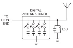
Figure 6 Digital antenna tuner example using a shunt switched capacitor bank.
Antenna Tuning
Another critical and rapidly evolving technology for next generation devices is antenna tuning. Switches can be applied for both on-antenna aperture tuning as well as the antenna-feed impedance tuning. Because these have very different characteristics, with some applications calling for high Q and low Ron, and others calling for minimum Coff, they must be optimized for the specific antenna structures being used. With these needs in mind, Skyworks delivers a variety of new antenna tuning products that bring value to OEMs. Skyworks’ product portfolio includes active antenna tuning solutions based on FET switching technology that allow improved impedance matching for a single antenna across a wider bandwidth. This reduces power stress on the transmitter side and increases sensitivity on the receiver side (see Figure 6).
Carrier Aggregation
Skyworks has also introduced breakthrough RF switching technology that is enabling early adopters to implement carrier aggregation solutions. Carrier aggregation allows mobile service providers to combine spectral bands, increasing data rate throughput by utilizing two or more bands simultaneously instead of the single band method used currently. This gives consumers an enriched data experience regardless of location. Skyworks’ devices support standardized inputs to popular industry chipsets (MIPI RFFE compatible) and address both transmit and receive switching paths. Skyworks’ carrier aggregation switching solutions are compliant to tier-one carrier-driven specifications, offer dedicated receive diversity functionality to accompany the primary antenna switch path, are based on SOI and PHEMT wafer process technologies, and are available in many different configurations.
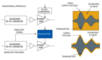
Figure 7 Envelope tracking vs. the traditional approach.
Envelope Tracking
Other ongoing challenges in the increasingly complex RF front end include improving power savings and talk time. Recent PAE improvements, including envelope tracking, help enhance performance since power amplifiers and associated components still consume a significant percentage of system power.
Envelope tracking enables the voltage supplied to the final RF stage power transistor to be changed dynamically and synchronized with the RF signal passing through the device. The supply voltage is reduced from its maximum value and is allowed to track the signal envelope, resulting in lower dissipated energy (see Figure 7). An envelope tracking amplifier operates at its optimum efficiency for all envelope levels, greatly improving efficiency when operating with envelope varying signals. Envelope tracking is expected to deliver 200 to 500 mW, or more, in battery power savings, along with 20 to 30 percent less dissipated power, lower heat dissipation, and improved 3G/4G coverage per base station since less back-off will be required.
Conclusion
Consumer demand for mobile platforms that are able to roam globally and interface seamlessly to any and all network topologies remains unabated and is demanding an unprecedented level of RF complexity. As a result, OEMs are seeking partners who can deliver front end solutions that preserve battery life, increase data rates, solve signal interference problems and occupy minimal board space. This need plays directly to Skyworks’ strengths and technology-agnostic approach. While others continue to bet on a singular architecture or process technology, and develop solutions that are convenient to their particular business models, Skyworks is investing in all core building blocks and specialized process technologies to deliver everything from best-in-class discrete products to complete system solutions. This approach gives customers maximum design flexibility for the highest performing solutions. Most importantly, it enables OEMs to focus on what’s important to their business models and in bringing highly innovative, next-generation platforms to market faster.