
Electromagnetic signals are used to transmit information in the form of amplitude, frequency, phase and time duration of an oscillation. In many cases, they must be amplified from a low to a higher power level by an amplifier having special basic characteristics, such as sufficient gain within a specific frequency band, low noise, stability, low power consumption and low cost. One of the approaches to satisfy the amplification requirements at microwave frequencies is to use a reflection amplifier.1 The development of such devices has been described previously.2-6 One of the basic problems in the development of a reflection amplifier is its relatively narrow frequency band as well as its low stability. In a previous publication,1 the authors proposed a reflection amplifier using a transistor with positive series feedback, showing a higher stability and efficiency than a reflection amplifier with parallel feedback. Later on, after more research, new results were obtained.7 In this article, as an extension of the previous work, a more detailed analysis is proposed for a reflection amplifier using mismatched resonant circuits.
The method of mathematical analysis of negative resistance is well defined,5,6,8,9 but the physical process of amplification to a higher power level is masked. In this article, simple physical concepts are provided to understand in detail the amplification process in this kind of amplifier. The design process of negative resistance amplifiers is very complex, giving only approximate results. Here, the analysis of reflection amplifiers is explained with the help of general concepts used in two-port amplifiers, allowing an easy design procedure.
Theory
Any amplifier contains an energy source (DC) and a controlled nonlinear element (diode or transistor). In a reflection amplifier, the DC source is energy transformed into RF power according to the input signal level S(t). Two basic circuits of the transistor reflection amplifier are shown in Figure 1 — (a) with a parallel positive feedback and (b) with a series positive feedback.
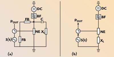
Fig. 1 Basic amplification schemes for a transistor reflection amplifier.
The circuit with parallel positive feedback is the most extensively studied. It contains a DC source, a nonlinear element (NE), a matched reactive load (XL), a circulator to separate the input signal (S(t)) and the output signal (POUT), positive feedback elements (FB), and additional blocking elements (bandpass filter BF and an output capacitance C). An example of this kind of reflection amplifier has been previously reported.2
The subject of this work is the study of the amplification phenomena of the amplifier working with a series positive feedback. The basic element of the circuit determining its principal parameters is a controlled nonlinear element (in this case a field effect transistor). An inductor with reactance XL and the internal nonlinear capacitance of the transistor compose the feedback circuit.
The amplification process of the reflection amplifier with different positive feedback schemes is shown in Figure 2. The equivalent circuit model of the FET transistor can be represented by two connected nonlinear elements — the area of the gate-channel represented by a Schottky barrier diode (D), working like a small-signal-controlled capacitance (Cg-ch) (varactor), and the area of the channel represented by a second diode, working like a controlled conductance Gds (or resistance Rds). The equivalent circuit with parallel positive feedback contains two signal sources Vs and VFB having equal phases and shifted by 2πn (n = 1,2,3, …) that work synchronously with the controlling element (D). The equivalent circuit with series positive feedback also contains two signal sources, but working synchronously and applied in series to D. The principal difference between the series and parallel feedback circuits is the phase shift between Vs and VFB. For the series circuit the phase shift is (2n+1)π, for n = 0, 1, 2, …. A more detailed explanation of the operation principle of a one-port transistor amplifier (OPTA) circuit with series feedback is shown in Figure 3.
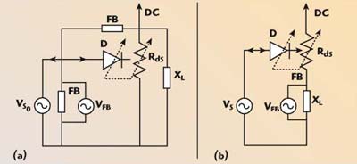
Fig. 2 Amplification process in a reflection amplifier with positive feedback; (a) parallel and (b) series.
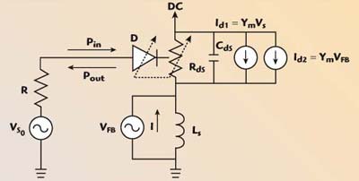
Fig. 3 The principle of operation for an OPTA.
When the circuit is turned on, energy storage occurs in the form of a magnetic field at the inductance Ls given by Equation 1.
E = 0.5I2Ls or power P = 0.5I2ωLs (1)
where
I = current flowing through the inductance Ls
ω = angular frequency
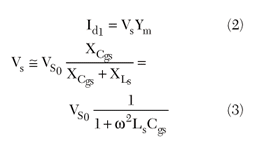
This value is the maximum limit of the output RF power, resulting a purely reactive energy. When the input signal (VS0) is applied to D, part of this voltage (Vs) modulates the channel resistance Rds that at the same time modulates the constant current of DC source. The modulated part Id1 of the channel current in this case can be obtained from
where
Ym = transistor transconductance
Cgs = gate-source capacitance
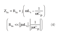
XCgs, XL = reactive components of the input impedance of the transistor given as
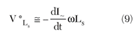
The interaction between the modulated current and the stored energy in the source inductance Ls, produces a self-induction voltage VLs
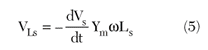
Ls is the source of the amplified signal and voltage for the positive series feedback, resulting in a voltage of feedback (VFB) that is applied to the cathode of D, generating an additional modulated channel current Id2 as
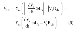
when
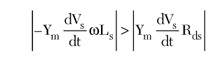
a positive feedback is obtained, otherwise a negative feedback exists.
The second current contribution Id2 is obtained by
![]()
The channel resistance modulation occurs with the help of two sources series connected and applied to the anode and cathode of the controlling diode D. As a result, at the input reference plane, both (the input and output) signals are present with opposite phases, reducing the possibility of a self-excitation.
Because Vs and VFB act synchronously on the channel resistance, the result is a total variable channel current
![]()
and a self-induction voltage
The amount of the variable total channel current will be determined by the DC current, the circuit losses and the power re-reflection at the input network.
The power dissipated at input load (R) is
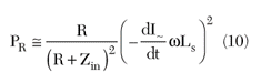
The output power is determined by the input signal and the amount of the feedback voltage produced by the source inductance and transconductance of the controlled nonlinear element. In an extreme case, the value of this power is limited only by the stored energy at the source inductance (Equation 1) and the circuit losses.
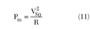
In this case the input signal power is given as
The proposed power transmission coefficient (gain) of the reflection amplifier at the reference plane of the transistor gate can be approximated by
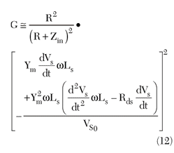
Substituting for the derivatives, a new expression for gain is obtained:
where the equation terms have been defined previously.
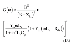
In order to verify the proposed expressions for gain calculation, the following example provides the calculated gain using Equation 13 for an L-band reflection amplifier using an HJ FET NE33284A transistor. The calculated gain is shown in Figure 4. The design of the parallel resonant circuits is performed to satisfy the required gain flatness characteristics within the frequency band.
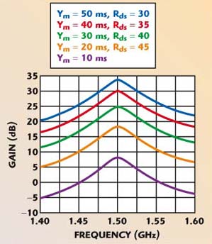
Fig. 4 Calculated gain for the L-band OPTA.
Experimental Results
Using both the theory given in the previous section and the MMICAD computer software, an OPTA with multiple resonant circuits has been designed for operation at L-band and is shown in Figure 5. A photograph of the OPTA circuit is shown in Figure 6.
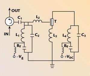
Fig. 5 Principal circuit elements of the reflection amplifier.
Fig. 6 The one-port transistor amplifier (OPTA).
The simplified amplifier circuit includes a circulator, a heterojunction FET transistor (T) with a transconductance (Ym), two series resonant circuits (C1, L2 and Cgs, L3) tuned at the center frequency and two parallel resonant circuits with a frequency tuning capability (L1, C2 and L4, C3). The main condition for the operation of the amplifier is to establish a series resonance of the transistor input capacitance (Cgs) with the source inductance (L3) at the center frequency. The main differences between the amplifier presented in the previous work1 and this article include the following: the tuning of the input matching circuit was made at one center frequency, and to increase the amplifier stability, the transistor drain terminal was RF blocked to ground.
The chosen active element is a GaAs heterojunction FET with a gate length Lg = 0.3 µm and a gate width wg = 280 µm. When operating in a two-port amplifier this device has a minimum noise figure = 0.3 dB and an associated gain = 19 dB at 1.5 GHz when biased at Vds = 2 V and Id = 10 mA (P = 20 mW). Otherwise, operating as a one-port amplifier, it is biased at Vds = 0.1 V and Id = 3 mA (P = 0.3 mW).7 Operating at this bias point, the power consumption is reduced drastically.
To calculate the principal characteristics, the selected transistor S-parameters and the transconductance have been measured previously. The value of the transistor source inductance (L3) was calculated to resonate at 1.5 GHz together with the gate-source capacitance (Cgs). The parallel resonant circuits at the gate and drain networks were calculated at the same frequency with a deviation of ±30 MHz. To separate the incident and reflected signals, a circulator operating in the 1.45 to 1.55 GHz frequency band has been used. This circulator has an insertion loss between –0.17 and –0.25 dB and an isolation better than –20 dB within the operating bandwidth.
The S-parameters and gain measurements were performed with a HP8510C network analyzer, as shown in Figure 7, and the noise figure was measured using a noise figure meter HP8970A in the 1.4 to 1.6 GHz frequency band. The measurement results for the OPTA can be seen in Figure 8, showing the change of gain characteristics at the bias conditions Vg = –0.5 V and Id = 3 mA for different values of the source inductance L3 ranging from 25 to 35 nH. It is worthy to mention that in order to find the optimum bias conditions to operate the OPTA, the drain current Id was adjusted for minimum noise figure and the gate voltage Vg was allowed to vary from –0.33 to –0.7 V.

Fig. 7 OPTA S-parameter measurements using a HP8510C network analyzer.
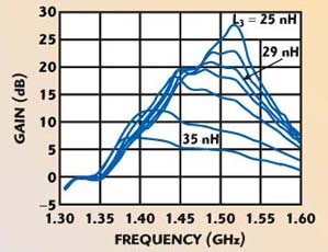
Fig. 8 Measured gain of the OPTA for different values of source inductance (L3).
The feature of this amplifier is that the input transistor impedance, with source inductance included, must be a purely active resistance at the center frequency. This condition will increase the stability of the amplifier and simplify the design of the input matching network.
Tuning the inductance L3 and fixing the Vds voltage at 0.1 V, the maximum gain flatness characteristic and low noise figure were obtained, as shown in Figure 9. In the same figure, the calculated gain according to Equation 13 is given for comparison.
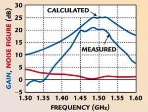
Fig. 9 Gain and noise figure for a fixed L3.
The values of the calculated and experimental gains were 25 and 20 dB, respectively. The wide disagreement between the calculated and measured gain can be explained by the effect of the re-reflections and losses at the input network due to the opposite phase between the input and output signals.
In addition, the measured isolation of the circulator at this frequency is –20 dB, and a better circulator, near the “ideal,” will improve the agreement between calculated and experimental results. The strong influence of the signal re-reflections at the input network is observed by connecting the amplifier to a T-junction instead of the circulator (see Figure 10). This graph shows also that the re-reflections at the input network affect the gain and transistor noise equally and indirectly justifies the validity of the expression for noise figure given in a previous publication.7
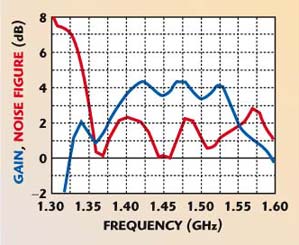
Fig. 10 Gain and noise figure of the OPTA with a T-junction.
Figure 11 shows the characteristics of the amplifier, where the obtained minimum noise figure is 0.5 dB, the associated gain is 20.5 dB ±0.5 dB, and the return losses at the input and output ports are better than –34 and –25 dB, respectively, within a bandwidth of 75 MHz and with a power consumption close to 0.3 mW. To estimate the efficiency for DC power consumption, the figure of merit as proposed by Kobayashi, et al.10 has been used. It is defined as the ratio of the gain (dB) to the power consumed (mW). The measured parameters demonstrated a very high performance for the figure of merit (> 65 dB/mW). For comparison, the best result up to date (19.1 dB/mW) in this frequency band was achieved by K.R. Cioffi.11
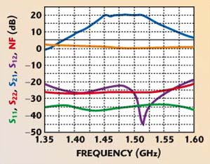
Fig. 11 Summary of the OPTA characteristics.
It must be emphasized here that the source inductance is a very important element to design a reflection amplifier with series positive feedback. The principal functions of this element are the accumulation of reactive energy in the form of magnetic field and the generation of a self-induction voltage that is the source of the series positive feedback. This voltage also creates the effect of “negative” resistance at the transistor input. It is the source element to provide an output signal at a high energy level.
Conclusion
In this article the operation principle of reflection amplifiers has been described as an alternative to conventional two-port amplifiers. The theoretical analysis of this kind of amplifier has been presented, and as a result, a new expression to estimate the gain in reflection mode amplifiers has been proposed. The results of a reflection amplifier with multiple resonant circuits for L-band operation were obtained. It is worthy to mention that the reflection amplifier design is very simple, since it is enough to know the principal electrical parameters of the selected transistor and have the appropriate circulator characteristics to calculate the reflection amplifier elements. The application of the proposed reflection amplifier gives enough stable characteristics and high power efficiency over a wide frequency band, in comparison with purely resonant circuit reflection amplifiers.
Acknowledgment
The work was supported by the Mexican National Council of Science and Technology CONACYT under grant: 41267-Y.
References
- A.P. Venguer, J.L. Medina, R.A. Chávez and A. Velázquez, “Low Noise One-port Microwave Transistor Amplifier,” Microwave and Optical Technology Letters, Vol. 33, No. 2, April 20, 2002, pp. 100–104.
- H. Tohyama and H. Mizuno, “23 GHz Band GaAs MESFET Reflection Type Amplifier,” IEEE Transactions on Microwave Theory and Techniques, Vol. 27, No. 5, May 1979, pp. 408–411.
- R. Zbinden, “The Reflection Amplifier Using the Microwave Transistor,” Mitteilungen AGEN Journal, ETH, Zurich, Switzerland, August 1980.
- F. Lenk, R. Doerner and R. Heymann, “Negative Resistance in GaAs MESFET Nonlinear Modeling,” INMMC 4th International Workshop on Integrated Non-linear Microwave and Millimeter-wave Circuits, Gerhard-Mercator University Duisburg, October 9-11, 1996, pp. 77–82.
- P. Gardner and D.K. Paul, “Aspects of the Design of Low Noise, Negative Resistance Reflection Mode Transistor Amplifiers,” IEEE Transactions on Microwave Theory and Techniques, Vol. 39, No. 12, November 1991, pp. 1869–1875.
- P. Gardner and D.K. Paul, “Optimum Noise Measure Configurations for Transistor Negative Resistance Amplifiers,” IEEE Transactions on Microwave Theory and Techniques, Vol. 45, No. 5, May 1997, pp. 580–586.
- A.P. Venguer, J.L. Medina, R.A. Chávez and A. Velázquez, “A New Microwave One-port Transistor Amplifier with High Performance for L-band Operation,” WSEAS International Conferences, Cancún, Mexico, CD-ROM Proceedings, May 12-16, 2002, pp. 2061–2066.
- R.G. Ranson and P. Huish, “Design of Reflection Amplifiers,” Microwave Solid State Devices and Applications, D.V. Morgan and M.J. Howes, Eds., Peter Peregrinus, Stevenage, UK, 1980, Chapter 10, pp. 134–145.
- J.L.S. Franco, “Amplificador por Reflexion de Banda Ancha en Microstrip,” Anuales de Fisica, Serie B, Vol. 82, 1986, pp. 79–86.
- K.W. Kobayashi and A.K. Oki, et al., “5 mW GaAs HBT Low Power Consumption X-band Amplifier,” IEEE International Microwave Symposium Digest, 1994, pp. 17–20.
- K.R. Cioffi, “Monolithic L-band Amplifier Operation at Milliwatt and Submilliwatt DC Power Consumption,” IEEE MMCS Digest, 1992, pp. 9–12.