
Base station applications for WiMAX require low noise amplifiers (LNA) with low noise figures, high linearity, compact size, and excellent input and output return loss.1 A balanced amplifier topology is often the preferred choice in LNA applications for base station transceiver front-ends, because it presents several advantages over single-ended amplifiers such as excellent input and output return loss, higher linearity and better stability.2 These requirements present several design challenges that involve technology and design trade-offs of couplers to achieve an optimal solution in terms of size and performance. GaAs E-PHEMT has an enormous potential for realizing low noise amplifiers at microwave frequencies, due to their low noise features, high electron velocity and positive gate bias voltage requirements.3
A branch line coupler is one of the most popular hybrids for the design and implementation of balanced LNAs.4 However, a branch line coupler requires a large circuit area, due to the quarter wavelength transmission lines.4 Various efforts to reduce the size of the branch line coupler have been reported.5-7 The Lange coupler8 is relatively impractical for fabrication on a printed circuit board (PCB) as the lines are very narrow, close together and is more practical for MMIC designs. The broadband lumped element 3 dB quadrature coupler9 is more suitable for MMIC applications. A branch line coupler is more suitable for base station LNAs because it has better input and output return losses and lower insertion loss, compared to the lumped element approach. In order to design a reduced size branch line coupler on a PCB for low cost applications, the design technique proposed by Ching-Wen Tang10 is more promising and hence chosen for this design.
Balanced LNA Design
The schematic of the proposed balanced LNA is shown in Figure 1. The design of a balanced LNA comprises two main steps. The first step involves the design of a single stage LNA. Once the single stage amplifier has been designed, the next step involves the design of an appropriate coupler to meet the size and bandwidth requirements.
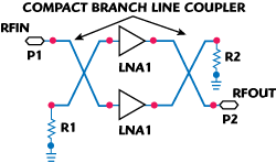
Figure 1 Simplified schematic of the proposed balanced LNA.

Figure 2 Schematic of the proposed LNA.
LNA Design
The Avago Technologies ATF-5414311 high dynamic range, low noise enhancement mode PHEMT (E-PHEMT) device was selected for the amplifier design. The schematic of the LNA is shown in Figure 2. A voltage divider, consisting of R1 and R2, is used to bias the FET. The purpose of R4 is to enhance the low frequency stability of the device by providing a resistive termination at low frequencies. The capacitor C3 provides a low frequency bypass for R4. Additional resistance in the form of R5 (approximately 10 kΩ) is added to provide current limiting for the gate of enhancement mode devices such as the ATF-54143. Quarter wavelength microstrip lines are used to provide the DC feed and to improve the capability of blocking the RF signal.
Radial stubs are used, together with the quarter wavelength microstrip lines, to improve the isolation of the DC and RF path.4 The LNA stability is improved by adding an inductance at the emitter (source) of the active device.12 Input impedance matching, using inductive source degeneration, is a popular approach, because matching to the source does not introduce additional noise (as in the case of using a shunt input resistor) and does not restrict the value of gm (as in the case of the common-gate configuration).

Figure 3 Simulated Γopt and noise circles.

Figure 4 Simulated Gp circles.
Input and Output Matching
For low noise applications, the input matching is done at Γopt to achieve the lowest noise possible.4 The maximum gain is achieved, for unconditionally stable amplifiers, when both input and output are conjugate matched. The results of Γopt and noise circles, calculated for the input matching design, are shown in Figure 3.
For output matching requirements, the GP circles calculated for various gain values are shown in Figure 4. In order to achieve the lowest LNA noise figure possible, the input stage of the amplifier is matched to Γoptt,4 the location of which is 36.127-j12.93 Ω. The matching network is designed to match 50 Ω to 36.127- j12.93 Ω. A single stub matching technique, using series and shunt open stubs, is selected to design the input matching network. The output matching network transforms the load impedance from 48.64 + j29.86 Ω to 50 Ω for a gain of 15 dB.

Figure 5 Equivalent circuit of a quarter wavelength transmission line.

Figure 6 Diagram of the T model microstrip branch line coupler using a low impedance approach.
Compact Branch Line Coupler Design
The size reduction of the branch line coupler is practical, using the approach proposed by Razavi.12 Figure 5 shows the equivalent circuit of the quarter wavelength transmission line. Three types of shortened quarter wavelength transmission line can be used for the compact branch line couplers. They are the T-model, the π-model and a combination of both models.12 The low impedance T-model approach is selected in this research, due to the ease of implementation and the reduced complexity in terms of layout. The design uses the low impedance open stub in the shortened quarter wavelength transmission line of the T-model. Figure 6 shows the T-model microstrip branch line coupler using the low impedance approach.
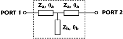
Figure 7 Equivalent quarter wavelength transmission line of T model.
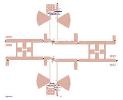
Figure 8 Layout of the balanced LNA using compact branch line couplers.
Using Equations 1 and 2, the impedance and lengths of each shortened equivalent quarter wavelength, which are Za, Zb, θa and θb as depicted in Figure 7, are derived for both the shunt and series arms. A size reduction of approximately 40 percent is reported using a compact branch line coupler. The complete design of the balanced LNA, using compact branch line couplers, is shown in Figure 8.

Figure 9 Simulated S-parameter results.

Figure 10 Measured S-parameter results.
Simulation and Measured Results
The simulated small-signal S-parameters, which includes the gain, input and output return losses and isolation, are shown in Figure 9. As can be observed, the maximum value of gain obtained is 14.74 dB at 2.3 GHz and rolls off gradually to 13.44 dB at 2.7 GHz. The input and output return losses are very good across a limited bandwidth, better than 10 dB from 2.3 to 2.7 GHz. The measured small-signal S-parameters are shown in Figure 10. Good agreement between the simulated and measured results can be observed. The measured gain is slightly lower, 14.30 dB at 2.3 GHz to 13.50 dB at 2.7 GHz. Both simulation and measured results show a gain flatness of less than 1 dB. The input and output return losses degraded slightly, compared to the simulated results. The reason for the deviation of a few dB is due to the losses in the microstrip elements of the amplifier and coupler circuits, variations in the SMD devices and coupling of signals between the amplifiers. The comparison between simulated and measured noise figure results is shown in Figure 11.

Figure 11 Simulated and measured noise figure.

Figure 12 Simulated and measured input IP3 results.
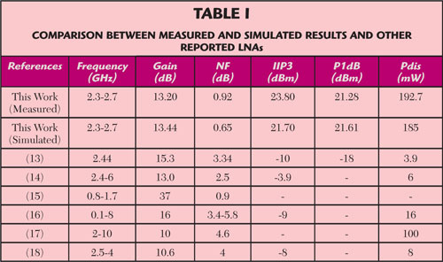
The noise figure measurements were made in a shielded room. The measured noise figure performance was found to degrade slightly, compared to the simulated noise figure of the circuit. However, the measured noise figure is well below 1 dB and only degrades approximately 0.2 to 0.3 dB from simulation. This low noise figure has been achieved by matching the input at Gamma Opt and using E-PHEMT device. The simulated noise figure is typically lower than the measured one, due to unaccounted sources of noise such as the noise contributed by the power supply and ambient noise. Figure 12 shows the simulated versus measured input IP3. The higher input IP3 is achieved using the balanced approach as compared to the single-ended design. Measurement and simulated results are summarized and compared with previous reports of LNA designs in Table 1. The complete fabricated device is shown Figure 13.

Figure 13 Photograph of the fabricated LNA.
Conclusion
A balanced LNA design, which uses compact branch line couplers, has been designed and developed. This LNA exhibits a small-signal gain of 14.30 dB at 2.3 GHz and 13.50 dB at 2.7 GHz. An output power of 21.28 dBm and an OIP3 of 37.2 dBm at 2.5 GHz have been obtained. Excellent noise figure performance below 1 dB is achieved across the bandwidth of interest. This design is suitable for applications that require a smaller size device. By using the compact branch line couplers, a size reduction of 40 percent is achieved as compared to using the conventional branch line coupler. Excellent performance could be achieved even by reducing the branch line coupler by almost 40 percent.
Acknowledgment
The author would like to thank the Universiti Kebangsaan Malaysia and USM for their support.
References
- WiMAX Forum: Fixed, Nomadic, Portable and Mobile Applications for 802.16-2004 and 802.16e WiMAX Networks.
- W.R. Deal, M. Biedenbender, P.H. Liu, J. Uyeda, M. Siddiqui and R. Lai, “Design and Analysis of Broadband Dual-gate Balanced Low Noise Amplifiers,” IEEE Journal of Solid-State Circuits, Vol. 42, No. 10, October 2007, pp. 2099-2106.
- O. Berger, “GaAs MESFET, HEMT and HBT Competition with Advanced Si RF Technologies,” 1999 GaAs MANTECH Proceedings, pp. 7-10.
- D.M. Pozar, Microwave Engineering, Second Edition, John Wiley & Sons Inc., Somerset, NJ, 1998.
- T. Hirota, A. Minakaw and M. Muraguchi, “Reduced-size Branch Line and Rat-race Hybrids for Uniplanar MMICs,” IEEE Transactions on Microwave Theory and Techniques, Vol. 38, No. 3, March 1990, pp. 270-275.
- R.W. Vogel, “Analysis and Design of Lumped- and Lumped-distributed Element Directional Couplers for MIC and MMIC Applications,” IEEE Transactions on Microwave Theory and Techniques, Vol. 40, No. 2, February 1992, pp. 253-262.
- H. Ghali and T.A. Moselhy, “Miniaturized Fractal Rat-race, Branch-line and Coupled-line Hybrids,” IEEE Transactions on Microwave Theory and Techniques, Vol. 52, No. 11, November 2004, pp. 2513-2520.
- J. Lange, “Interdigitated Strip-line Quadrature Coupler,” IEEE Transactions on Microwave Theory and Techniques, Vol. 17, No. 12, December 1969, pp. 1150-1151.
- Y.C. Chiang and C.Y. Chen, “Design of a Wideband Lumped-element 3 dB Quadrature Coupler,” IEEE Transactions on Microwave Theory and Techniques, Vol. 49, No. 3, March 2001, pp. 476-479.
- C.W. Tang and M.G. Chen, “Synthesizing Microstrip Branch-line Couplers with Predetermined Compact Size and Bandwidth,” IEEE Transactions on Microwave Theory and Techniques, Vol. 55, No. 9, September 2007, pp. 1926-1934.
- ATF-54143 Low Noise Enhancement Mode Pseudomorphic HEMT in a Surface Mount Plastic Package.
- B. Razavi, RF Microelectronics, First Edition, Prentice Hall, Upper Saddle River, NJ, 1998.
- M. Cimino, H. Lapuyade, Y. Deval, T. Taris and J.B. Bégueret, ”Design of a 0.9 V, 2.45 GHz Self-testable and Reliability-enhanced CMOS LNA,” IEEE Journal of Solid-State Circuits, Vol. 43, No. 5, May 2008, pp. 1187-1194.
- J.Y. Hsieh, T. Wang and S.S. Lu, “Wideband Low Noise Amplifier by LC Load Reusing Technique,” Electronics Letters, Vol. 45, No. 25, December 2009, pp. 1278-1280.
- Z.X. Wang, Y.W. Ming, P.J. Hong, C.J. Xin, X.W. Bo and S. Chen, “The Design of SIGE HBT Balanced Broadband Low Noise Amplifier,” 2008 Beijing Microwave and Millimeter Wave Technology Digest, pp. 233-236.
- T.Y. Chang, J.H. Chen, L. Rigge and J.S. Lin, “A Packaged and ESD Protected Inductorless 0.1 to 8 GHz Wideband CMOS LNA,” IEEE Microwave and Wireless Components Letters, Vol. 18, No. 6, June 2008, pp. 416-418.
- X. Guan and C. Nguyen, “Low Power Consumption and High Gain CMOS Distributed Amplifiers Using Cascade of Inductively Coupled Common Source Gain Cells for UWB Systems,” IEEE Transactions on Microwave Theory and Techniques, Vol. 54, No. 8, August 2006, pp. 3278-3283.
- S.C. Blaakmeer, E.A.M. Klumperink, D.M.W. Leenaerts and N. Bram, “A Wideband Noise Canceling CMOS LNA Exploiting a Transformer,” 2006 IEEE Radio Frequency Integrated Circuits Symposium Digest, pp. 137-140.