If amplifiers are used in many applications, including base stations, cable TV and instrumentation. High linearity is one of the most desired features of an IF amplifier. New applications, such as amplifiers used in cable TV, also require very flat gain and low noise. Darlington amplifiers with single or dual RF feedback topologies have been shown to have higher gain, flatness and linearity over a wide bandwidth.1,2 Various device process technologies, including HBT, SiGe and PHEMT among others, have been used in the past. Each technology has its unique advantages. Different active, dynamic and passive biasing techniques have also been used to improve performance over temperature and over the frequency band of operation.3,4 Capacitive peaking techniques are used to further increase the bandwidth, with a trade off in input and output return loss.5 The drawback in most high linearity designs is the big trade off in noise figure (NF).
The design of a high linearity Darlington RF feedback amplifier with less than 2 dB NF has been achieved. The design uses a source capacitive peaking technique for optimum gain flatness across a wide band. Source degeneration inductors are used for improving the input and output return loss and stability at lower frequencies. Additional stability improvement circuits are used to ensure unconditional stability at higher frequencies.
Circuit Design
The frequency range of operation is from 30 to 1000 MHz. With a Darlington design topology, the first and second stages can be biased at different conditions. Individual voltage and current adjustment of each stage provides extra flexibility for performance optimization. The Darlington configuration provides twice the gain bandwidth product over single stage circuit topologies. Furthermore, good input and output return loss across a wide frequency range can be achieved with RF feedback optimization.
The IP3 can be further improved by presenting different impedance terminations to the device.6 When more voltage and current are available, the drain voltage and current can be increased to improve IP3 and the 1 dB compression point (P1dB) with minimal impact on other performance parameters.
The device process used in this design is a depletion (D)-mode low noise pseudomorphic high electron mobility transistor (PHEMT) with a thin film resistor (TFR). The PHEMT process inherently has low noise and very high linearity. This makes it suitable for this specific application. However, the design shown in this article is not limited to this type of process.

Figure 1 Die circuit schematic.
Figure 1 shows the circuit schematic of the die. Resistors at the sources (R4 and R6) are used to set the positive source DC voltage and the drain currents. The value of these resistors can be easily calculated using the current equation

where the gate-to-source voltage (VGS) and the pinch-off voltage (Vp) values are both negative. Once the drain bias current (IDS) is determined, VGS can be calculated. The gate voltage is chosen to be small. It is applied through the resistive divider (R1 and R2) and a very large value of shunt resistor (R3) connecting to the gate. Given the gate voltage, the source voltage and resistor can be calculated. The total current consumption is 100 mA at 5 V supply voltage. It is also important to consider the thermal design of the output transistor. For this reason the LNFET device layout is optimized using thermal calculators.
Two of the design constraints, NF and input return loss, are the main factors in determining the first stage design. An optimum device sizing and inductive degeneration technique are used for simultaneously optimizing noise figure and input match. The second stage is designed for optimum IP3 performance. The biasing conditions for each stage are crucial in determining the best overall IP3. One can choose the optimum biasing conditions such that second-order and third-order intermodulation products are cancelled.6
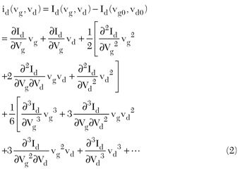
The drain current is controlled by the gate and drain voltages. In the small-signal case, it can be represented by a two-dimensional Taylor series expansion as an incremental drain current7,8

where Vg0 and Vd0 are the DC bias voltages and vg and vd are the small-signal gate and drain voltages.
If the higher order terms are ignored and the coefficients simplified, the small-signal incremental drain current can be written as

where the coefficients gm, g'mand g"m are the transconductance and its first and second derivatives with respect to vg.

Gd, G'd and G"d are the drain-to-source transconductance and its first and second derivatives with respect to vds.

And m11, m12 and m21 are cross terms defined as

The drain to source transconductance, in the saturation region where Vds is high, can be assumed to be small. The cross terms above are also generally small and can be ignored. Therefore, the id equation above can be further simplified to

The above equation gives rough guidance for optimizing the second-order intercept point (IP2) and IP3. It shows that the lowest second-order and third-order distortion products are achieved when the first and second derivatives of transconductance, g'mand g"m, are minimized. It is ideal to have both IP2 and IP3 products lowered. This can be accomplished by carefully selecting the bias points as well as optimizing the amplifier transconductance profile over a wide bias range. The analysis above also shows the sensitivity of this method to wafer uniformity and gain profile. The sensitivity can be reduced by process parameters9 as well as topology selection and feedback techniques.2
The Darlington topology with source degeneration allows gain optimization and high linearity. Capacitors C1 and C2 on the die are chosen for achieving the best gain flatness without seriously degrading input and output return losses. These capacitors are also used to bypass the source resistors and hence improve the NF. R1 and R2 on the die are used for setting the gate voltages.

Figure 2 Evaluation board schematic.
Figure 2 shows the test board schematic with external components. The external RF feedback resistor, R2, is chosen for the best input and output return losses and gain trade-off. C1, C2 and C4 are used for DC blocking.
Design for Stability
Typical specifications dictate unconditionally stable operation up to 18 GHz. This amplifier is designed for unconditionally stable operation, including the external components and biasing under all conditions. For this purpose, various stability design techniques have been employed and integrated into the amplifier. In order to solve stability problems at low to operating frequencies, a source inductor of some value is often used.
Component Selection Considerations
External feedback circuit components R2 and C2 can be tuned if a gain adjustment is needed. The input and output matching networks are composed of L1 and L2, respectively. The input and output matching circuits are designed to be centered at approximately 700 to 1200 MHz. This can also be tuned by the external matching components L1, C1 and L2, C4.

Figure 3 Noise figure vs. frequency.

Figure 4 Small-signal gain vs. frequency.
Measurement Results
An amplifier was fabricated and tested on the test board shown previously with a supply voltage Vdd of 5 V and a total supply current Id = 100 mA. Figure 3 shows the measured noise figure in a bandwidth of 30 to 1030 MHz. The input connector and board trace are not de-embedded from the measurement. The loss of the input transmission line was measured as 0.1 dB in this band. The NF is measured as approximately 2 dB from 100 to 1000 MHz, including the input transmission line loss. Figure 4 shows the measured amplifier gain as a function of frequency at several temperatures with an input power of -20 dBm. The gain is measured to be 15.6 dB at 450 MHz. The plots show that the gain changes less than 1 dB across the whole temperature range of -40° to 85°C.

Figure 5 Input return loss.

Figure 6 Output return loss.
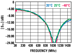
Figures 5 and 6 show the measured input and output return losses, respectively, with an input power of -20 dBm. The output third-order intercept point (OIP3) measured within the operating band was above 43 dBm. The OIP3 measurements were done using two signal sources with frequencies of 433.25 and 449.25 MHz at Pout = 5 dBm per tone.
Conclusion
Many performance aspects must be considered in the design of IF amplifiers. The next generation IF amplifiers require careful topology selection and competitive design techniques to meet the increasing demands of future applications. An optimized IF amplifier design, using a depletion mode PHEMT technology, is discussed in this article. It will be required to meet the challenging performance requirements of new circuit applications.
References
- R.G. Meyer and R.A. Blauschild, “A 4-term Wideband Monolithic Amplifier,” IEEE Journal of Solid State Circuits, Vol. 16, No. 6, December 1981, pp. 634-638.
- C.T. Armijo and R.G. Meyer, “A New Wideband Darlington Amplifier,” IEEE Journal of Solid State Circuits, Vol. 24, No. 4, August 1989, pp. 1105-1109.
- K.W. Kobayashi, “High Linearity Wideband PHEMT Darlington Amplifier with +40 dBm IP3,” 2006 Asian-Pacific Microwave Conference Proceedings, pp. 1035-1038.
- K.W. Kobayashi, “High Linearity Dynamic Feedback Darlington Amplifier,” 2007 IEEE Compound Semiconductor Integrated Circuit Symposium Digest, pp. 1-4.
- C.C. Meng, T.H. Wu and S.S. Lu, “28 dB Gain DC-6 GHz GaInP/GaAs HBT Wideband Amplifier with and without Emitter Capacitive Peaking,” 2002 Gallium Arsenide Applications Symposium.
- S.A. Maas, Nonlinear Microwave Circuits, IEEE Press, Piscataway, NJ, pp. 349-351.
- A.M. Crosmun and S.A. Maas, “Minimization of Intermodulation Distortion in GaAs MESFET Small-signal Amplifiers,” IEEE Transactions on Microwave Theory and Techniques, Vol. 37, No. 9, September 1989, pp. 1411-1417.
- G. Qu and A.E. Parker, “Intermodulation Cancellation in HEMTs,” 1998 International Conference on Microwave and Millimeter Wave Technology Proceedings, pp. 84-87.
