
There has recently been an exponential growth in worldwide wireless communications. The IEEE 802.11 group has been responsible for setting up standards, including those for wireless local area networks (WLAN), and dual-band communication at 2.4 GHz (2400 to 2483.5 MHz) and 5.2 GHz/5.8 GHz (5150 to 5350 MHz and 5725 to 5825 MHz). In particular, printed dipole-type antennas exhibit many attractive features, such as a simple structure, excellent pattern, easy integration with monolithic microwave integrated circuits (MMIC) and low radiation losses. The design for a planar dual-band dipole antenna with chamfers for dual-band resonances at 2.4 and 5 GHz has been described.1
In addition, a planar open-sleeve dipole (ELPOSD) and an end-load planar open-sleeve dipole antenna (ELPOSD) with parasitic elements2 have been designed and their increased bandwidth and length reductions have been demonstrated. An ultra-wideband printed dipole antenna3 with a tapered slot feed has been proposed and a broadband bandwidth from 3.1 to 10.6 GHz was obtained. The distance from the parasitic element to the feeding aperture adjusts the impedance matching. A broadband printed dipole antenna with an asymmetrical radiating patch operating in the DTV band was also shown.4 The dual-band operation of a printed dipole antenna5 with U-slotted arms has also been presented. The operating bands are 2.4/5.2 GHz WLAN bands for IEEE 802.11a/b. A CPW-fed monopole antenna with parasitic elements was used to generate wideband characteristics.6 The gap between the parasitic element and ground plane was an important parameter affecting impedance matching. In addition, microstrip-fed dipole antennas7-9 possess various advantages, such as a wide impedance bandwidth, low profile, easy manufacture and low cost.
A printed microstrip-fed dipole antenna7,8 is created using a small patch etched on the ground plane. The dual-band bandwidth of a microstrip-fed dipole antenna corresponds to the frequency range in IEEE 802.11.a/b. To achieve triple-frequency operation, a microstrip-fed dipole antenna using two parasitic elements as additional resonators was demonstrated.9 These studies indicate that planar dipole-type antennas with parasitic elements have various advantages, such as a wide bandwidth, low profile and compact size.

Figure 1 Geometry of the proposed dipole antennas: (a) rectangular arms, (b) rhombic arms, (c) rhombic arms and parasitic elements with slits.
This article proposes some designs for a dual-band and broadband planar dipole-type antenna with parasitic elements. The symmetrical parasitic elements were able to produce a resonant mode. By integrating the parasitic elements into the rectangular dipole antenna, a dual-band operation was realized. Further, by changing the radiation elements by adding a rhombic shape, broadband operation could be obtained. For WLAN application, a broadband antenna embedding L-shaped slits at the proper locations in the parasitic elements could produce a band-rejection characteristic. The novel design of the rhombic dipole antenna with parasitic elements is suitable for application in the WLAN (2.4 to 2.4835, 5.15 to 5.825 GHz) bands. Detailed design configurations for the proposed antennas are described. The results of the fabricated antennas are also presented and discussed.
Antenna Configuration and Design
Figure 1 depicts the geometry of a dipole antenna with parasitic elements. The antenna was designed on an FR4 substrate with a dielectric constant εr = 4.4, a thickness H = 0.8 mm and an overall compact size of Wsub (mm) × Lsub (mm). In the z-direction, the feed gap G is between the two antenna arms. The two arms of the antenna have the same width Wf and length Lf. The length Lf can be used to determine the first resonance mode. To increase the resonant modes, symmetrical parasitic elements were embedded beside the rectangular dipole arms. The two rectangular parasitic elements are placed on the substrate, symmetrically on either side of the antenna arms with a gap Ws, and have dimensions of W1 (mm) 3 L1 (mm).

Figure 2 Measured return loss of the rectangular arm dipole antenna: (a) as a function of L1 and (b) as a function of W1.
With the gap width G fixed at 0.5 mm, a good impedance matching was obtained. The parasitic elements are coupled to the dipole arms to generate a new resonant band. The operating frequency is varied with the length L1. Therefore, a dipole antenna with parasitic elements for dual-band operation is formed. When a rhombic-shaped plate was used to replace the two ends of the rectangular dipole arms of the printed dipole antenna, it was possible to generate a broadband characteristic such as the one described by Zhang and Spence.1,2
The figure shows the planar rhombic arm dipole antenna with the parasitic elements. It could produce a wider bandwidth performance. A rhombic shape was selected for the radiation plate with a dimension R1 = 9.9 mm. It reduced the total length of the antenna structure and lowered the resonant frequency in comparison with rectangular arms. The dipole antenna with the rhombic arms could generate a lower frequency band and a higher frequency band when coupled with the parasitic elements to enhance the operating bandwidth.
The figure also shows the planar rhombic arm dipole antenna with the parasitic elements embedded with two anti-symmetrical L-type slits. To decrease the interference between the WLAN and existing wireless systems, a broadband antenna with a band-rejection characteristic should be used. In this study, the total length of the slits (S1+S2) in the parasitic elements was selected as 10 mm with a width W2 = 1 mm, which could generate a band-rejection characteristic at 4.2 GHz. This total length was approximately a quarter-wavelength of the center frequency of the rejected band. The gap Sg between the slit and the feeding-line was used to adjust the impedance matching of the higher band to IEEE 802.11a. Thus, with the lower and higher operating bands obtained, a dual-band rhombic arm dipole antenna for IEEE 802.11a/b was achieved.

Figure 3 Measured return loss for the rhombic arm dipole antenna for different L1.
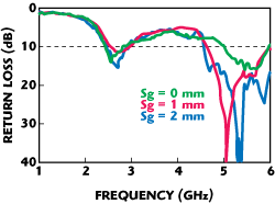
Figure 4 Measured return loss of the rhombic arm dipole antenna with slits as a function of the gap Sg.
Experimental Results and Discussions
Some antennas were fabricated to examine their performance. Figure 2 depicts the return loss with different lengths and widths for the parasitic elements in the rectangular arm antenna, with the other dimensions set at Lsub = 41 mm, Wsub = 15 mm, Ws = 0.5 mm, Wf = 2 mm, Lf = 23 mm and G = 2 mm. It was found that the second resonance mode shifts to a lower frequency as the length L1 increases, and that the length L1 of the strip is approximately a quarter-wavelength at the center resonant frequency in free space. As the width W1 is increased from 4 to 6 mm, the impedance matching at the higher-band gradually improved. Figure 3 shows the return loss in terms of various lengths for L1, for the antenna with rhombic arms, with the other dimensions set at Lsub = 41 mm, Wsub = 15 mm, W1 = 6 mm, Ws = 0.5 mm, Wf = 2 mm, G = 2 mm and R1 = 9.9 mm.
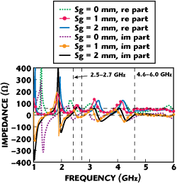
Figure 5 Measured impedance of the rhombic arm dipole antenna with slits as a function of Sg.
The second resonance frequency was affected by the length of the parasitic elements. It was observed that by using the rhombic arms in the antenna structure, a wideband operation from 2.37 to 8.33 GHz could be achieved (for a VSWR £ 2.5). Embedding a slit in the parasitic elements was also studied and is discussed below. The measured return loss, in terms of gap Sg, between the slit and feeding line is shown in Figure 4, with the other dimensions set at Lsub = 41 mm, Wsub = 15 mm, W1 = 6 mm, Ws = 0.5 mm, Wf = 2 mm, L1 = 13.mm, G = 2 mm, Sg = 2 mm, S1 = 8 mm and S2 = 2 mm and R = 9.9 mm.
Figure 5 shows the measured impedance versus frequency. The results show that varying the size of the gap Sg affects the higher band impedance matching. A larger gap Sg can result in improved impedance matching for the antenna’s higher band. This behavior is due to the generation of a higher resonance mode from the coupling between the feeding line and the symmetrical parasitic elements. The gap change will also affect the magnitude of the reactance. Therefore, a dual-band rhombic arm dipole antenna with parasitic elements is formed.
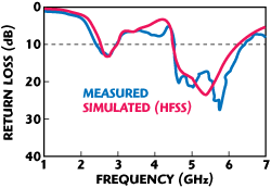
Figure 6 Measured and simulated return loss of the rhombic arm dipole antenna with parasitic elements with slits.
Figure 6 shows that there was good agreement between the measured and simulated return losses for the proposed antenna. The final antenna dimensions were Lsub = 41 mm, Wsub = 15 mm, W1 = 6 mm, Ws = 0.5 mm, Wf = 2 mm, L1 = 13 mm, G = 2 mm, Sg = 2 mm, S1 = 8 mm, S2 = 2 mm and R1 = 9.9 mm. The proposed dual-band operating bandwidths are from 2.4 to 2.92 GHz (19.5 percent) and 4.5 to 6.4 GHz (36.4 percent), which covers the IEEE 802.11 a/b/g bands.

Figure 7 Measured and simulated radiation patterns for the proposed antenna.
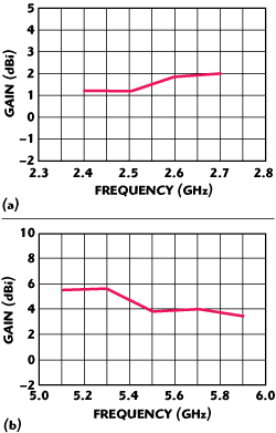
Figure 8 Measured antenna gain for the proposed antenna: (a) 2.4 to 2.7 GHz and (b) 5.1 to 5.9 GHz.
Figure 7 plots the measured and simulated radiation patterns at 2.45 and 5.5 GHz. In the X-Y plane, good omni-directional radiation patterns were obtained. It could be observed that coupling between the parasitic elements and the rhombic dipole arms led to a slightly directional cross-polar pattern. In the Y-Z plane, the co-polar pattern is donut-like. Although the two slits embedded in the parasitic elements had slight effects on the radiation patterns, they were acceptable for most wireless applications. Figure 8 shows the measured antenna peak gains against frequency. The measured gain variation in the lower operating band of 2.4 to 2.7 GHz was from 1.18 to 1.95 dBi; in the higher operating band of 5.1 to 5.9 GHz it was from 3.51 to 5.63 dBi. This represents gain variations of less than 3 dB. As seen in these results, the proposed dipole antenna has good impedance matching and excellent radiation characteristics.
Figure 9 shows the simulated current distribution using the HFSS for the dual-band antenna at 2.6, 4.2 and 5.5 GHz, respectively. It can be observed that the current is mainly focused on the rhombic dipole arms to generate a lower resonant frequency of 2.6 GHz. This allowed the antenna to easily cover the IEEE 802.11b band (2.4 to 2.4835 GHz). At 4.2 GHz, the current is seen on the side of the quarter-wavelength slit in the parasitical patch, which represents a band-rejection characteristic. At 5.3 GHz, the two parasitic elements affect the electromagnetic coupling with the feed-line, which leads to the generation of a new resonance mode at IEEE 802.11 a (5.15 to 5.35, 5.725 to 5.825 GHz).

Figure 9 Simulated surface current distribution of the proposed antenna: (a) 2.6 GHz, (b) 4.2 GHz and (c) 5.3 GHz.
Conclusion
A novel design has been proposed for a printed rhombic arm dipole antenna with parasitic elements and a band-rejection characteristic for dual-band WLAN applications. This was fabricated with a compact size of only 15 × 41 mm. To obtain a larger bandwidth, the coupling between the parasitical patches and feeding line was optimized by parameter analysis. This broadband antenna can be applied to wireless applications. Furthermore, a broadband antenna with two narrow inverted-L slits embedded in the parasitic elements yielded a band-notch characteristic. A dual-band operation from 2.4 to 2.92 GHz and 4.5 to 6.4 GHz and with good radiation performance was obtained. The proposed antenna should be attractive for WLAN applications.
- References
Z. Zhang, M.F. Iskander, J.C. Langer and J. Mathews, “Dual-band WLAN Dipole Antenna Using an Internal Matching Circuit,” IEEE Transactions on Antennas and Propagation, Vol. 53, No. 5, May 2005, pp. 1813-1818. - T.G. Spence and D.H. Werner, “A Novel Miniature Broadband/Multiband Antenna Based on an End-loaded Planar Open-sleeve Dipole,” IEEE Transactions on Antennas and Propagation, Vol. 54, No. 12, December 2006, pp. 3614-3620.
- T.G. Ma and S.K. Jeng, “A Printed Dipole Antenna with Tapered Slot Feed for Ultra-wideband Applications,” IEEE Transactions on Antennas and Propagation, Vol. 53, No. 11, November 2005, pp. 3833-3836.
- Y.W. Chi, K.L. Wong and S.W. Su, “Broadband Printed Dipole Antenna with a Step-shaped Feed Gap for DTV Signal Reception,” IEEE Transactions on Antennas and Propagation, Vol. 55, No. 11, November 2007, pp. 3353-3356.
- C.M. Su, H.T. Chen and K.L. Wong, “Printed Dual-band Dipole Antenna with U-slotted Arms for 2.4/5.2 GHz WLAN Operation,” Electronics Letters, Vol. 38, No. 22, October 2002, pp. 1308-1309.
- K. Chung, T. Yun and J. Choi, “Wideband CPW-fed Monopole Antenna with Parasitic Elements and Slots,” Electronics Letters, Vol. 40, No. 17, August 2004, pp. 1038-1040.
- H.M. Chen, J.M. Chen, P.S. Cheng and Y.F. Lin, “Feed for Dual-band Printed Dipole Antenna,” Electronics Letters, Vol. 40, No. 21, October 2004, pp. 1320-1322.
- J.P. Zhang, Y.S. Xu and W.D. Wang, “Ultra-wideband Microstrip-fed Planar Elliptical Dipole Antenna,” Electronics Letters, Vol. 42 , No. 3, February 2006, pp. 144-145.
- K. Chang, H. Kim and Y.J. Yoon, “A Triple-band Printed Dipole Antenna Using Parasitic Elements,” Microwave and Optical Technology Letters, Vol. 47, No. 3, November 2005, pp. 221-223.
Wen-Shan Chen received his BS degree in electronic engineering technology from the National Taiwan Institute of Technology (now National Taiwan University of Technology) and his PhD degree from National Sun Yat-Sen University, Kaohsiung, Taiwan, ROC, in 2001. From 2001 to 2002, he was an assistant professor at Chien-Kuo Institute of Technology, Changhua, Taiwan, ROC. He is currently an associate professor in the department of electronic engineering at Southern Taiwan University (previously Southern Taiwan University of Technology), Yung-Kang, Taiwan, ROC. His research interests include antenna design, RF and microwave circuits.
Yen-Hao Yu received his BS degree from Chung Hua University, Taiwan, ROC, in 2006. He is currently studying for his master’s degree in the department of electronic engineering, Southern Taiwan University. His areas of interest include printed antennas for wireless communications, especially for UWB and WiMAX applications.