
Many major RF component suppliers are offering integrated RF front-end modules (FEM), which are rapidly being adopted in today’s cell phones.
This is due to the fact that handsets do not merely make phone calls anymore; rather they are multimedia systems to be used for taking photos, playing video, games, music, e-mail and surfing the Web. This additional functionality results in less space for the radio front-end, which itself is trending towards increasingly complex multi-band/multi-mode operation. The RF front-end consists of several main building blocks: transceivers, power amplifiers (PA), duplexers (for CDMA/WCDMA systems) and switches (for GSM systems). Various strategies of system-in-package integration in the market include PA plus duplexers, PA plus switches, multiple blocks of filters/duplexers (multiplexers) and switch plus filters (such as antenna switch modules or ASM).1 CDMA phones are adopting multiplexers and PA and duplexer FEMs, while GSM/WCDMA phones make more use of the PA plus switches and ASM FEMs.1,2 Each integrated solution presents its own unique performance value proposition, but all offer common size reduction and quicker time-to-market. The integrated solutions produce shorter design cycles because they already handle the interactions between the discrete components such as matching and loading and simply have fewer RF components to put together. This article discusses specifically the multiplexer integration solution: what is it, what is needed to make a good one, provides several examples and speculates on future trends.
What is a Multiplexer?
A multiplexer is a device that combines multiple frequency band inputs onto a single antenna output. The advantage of this integration strategy is that it uses the same technology, so filter companies are able to parlay their expertise rather than combine unfamiliar technologies together. One clear advantage of a single antenna output is the elimination of additional antennas, which saves hardware cost to the manufacturer. Many examples exist in the worldwide market today, including triplexers and quintuplexers (PCS/Cellular/GPS) for the US market, quadruplexers (WCDMA Band 1+KPCS) for the Korean market and hexaplexers (WCDMA Bands 1,6,9) for the Japanese market.1–3
There are three main advantages to using multiplexers: size, performance and speed of integration. Substantial PCB space reductions of up to 70 percent could be realized, while routing and matching losses are reduced or eliminated, improving performance. The improved insertion loss performance is becoming increasingly important in the receive chain, due to the industry migration towards cheaper CMOS chipsets that have worse noise figure and sensitivity and in the transmit chain, due to all the new functionality, which increases power consumption. The ability to drop a single known-good-module onto a phone board rather than integrating many discrete components is attractive as a time saving in the phone design cycle and has improved final phone test yield.
What are the disadvantages? Careful design of the I/O lines and grounding on the phone will be necessary when implementing this solution because the I/O pads are closely spaced and prone to cross talk, which then results in poor sensitivity. Sensitivity should not be an issue with proper PCB design. Since multiplexers are still a relatively new concept, securing multiple sources with expertise in the manufacturing of multiplexers could also be a difficulty. Lastly, antennas for certain duplexer combinations (such as WCDMA Bands 1,4,5) are quite difficult to design and build.
The two main schemes to enable a single antenna output in multiplexers are active switches or passive lumped element (LC) matching circuits. Both schemes serve the same purpose, that is to make the other duplexers/filters look like open circuits while allowing signals in the frequency band of interest to reach the antenna. The advantage of the lumped element matching circuit is that it allows for simultaneous operation of multiple bands, eliminates the need for the control lines needed for switches and provides significant additional wideband rejection. This functionality is very attractive for new CDMA phones, which today use simultaneous GPS operation to comply with the E911 mandate from the FCC. Both triplexers and quintuplexers utilize this totally passive method and are adopted in a majority of new US phones.
Switches are needed when bands overlap, such as in the 1,2,5 WCDMA world phone bands (Band 1 Tx is 1920 to 1980 MHz and Band 2 Rx is 1930 to 1990 MHz), which makes it impossible to use the LC approach. In Japan, switches are used in essentially all the tri-band WCDMA phones because that specific phone architecture demands three different outputs (two for voice/data and one test port).
ASM modules have been widely adopted in the GSM world, integrating quad-band GSM Rx filters and switches together. ASMs are now adding on WCDMA ports, but not yet integrating the duplexers within. Switch integration has been accomplished either as a discrete module soldered onto a motherboard or buried into the LTCC cavity substrate.
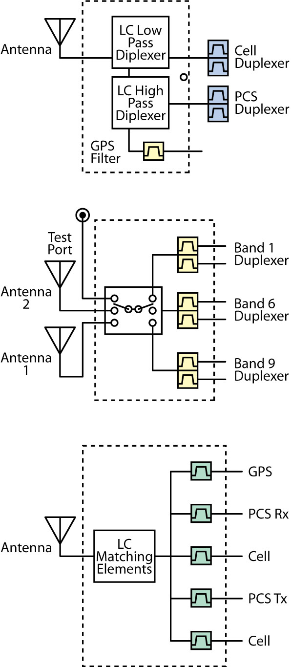
Figure 1 illustrates different levels of integration for the various multiplexers on the market. The blue color identifies the off modules discrete duplexers; the yellow, discrete filters/duplexers soldered onto the multiplexer motherboard; and the green, the filters mounted on the motherboard. The first level of integration is illustrated with the triplexer (3.2 x 3.2 x 1.6 mm).
The triplexer implements the LC matching elements integrated in the LTCC substrate with a GPS filter mounted on top while keeping the PCS and cell band duplexers separate as discrete components. This method has maximum flexibility for the phone manufacturer to use multiple suppliers. However, board space usage is higher because three separate components are used to accomplish the filtering.
The second level of integration is to solder the discrete duplexers/filters all on a single motherboard. In Japan, the hexaplexers have three discrete SAW duplexers mounted onto a common motherboard with footprints as small as 6 x 5 x 1.2 mm. Japan has the highest level of WCDMA adoption in the world with tri-band WCDMA operation commonplace.
While the size of discrete duplexers is shrinking, currently at 3 x 2.5 mm and with a next target footprint of 2.5 x 2 mm, the size of this type of multiplexer will be limited by the ability of discrete duplexers to shrink. The third and highest level of integration can be seen in the quintuplexer (5 x 8 x 1.2 mm), shown in Figure 2, where the matching and wafer level packaged filters are all integrated onto a single PCB. There are five FBAR die and three capacitors die mounted onto the multiplexer substrate. 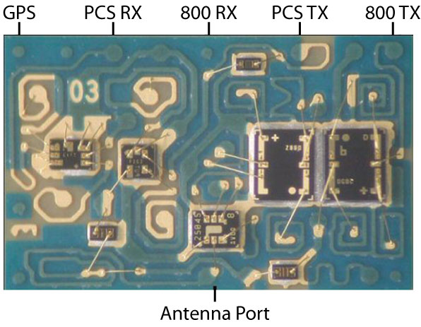
This provides the maximum level of reduction in x, y and z dimensions of the module and should be the trend as filter integration continues. Currently only film bulk acoustic resonators (FBAR) and solidly mounted resonator (SMR) bulk acoustic wave (BAW) are conceptually able to create modules with this level of integration as they already have demonstrated wafer level packaging technologies (microcap for FBAR and bump SiP for BAW) to assure hermeticity.7,8 Surface acoustic wave (SAW) filters do not yet have wafer level packaging capability and thus are limited to the previous two levels of integration; although a new type of wafer level packaged SAW filter, called interface acoustic wave (IAW), has been demonstrated in literature and could be not far behind commercially.9 Achieving this level of integration is challenging for several reasons.
First, all the individual building blocks need to be available. Then, actually integrating them together requires an accurate EM simulation to successfully control all the interactions of the closely placed of LC components and wire bonds on the module. Finally, and not to be underestimated, is the concatenated yield loss created by putting several duplexers/filters together all on a single PCB.
Building a Better Multiplexer
Building good multiplexers relies on good filter components. The qualities to look for in a good filter include high Q, access to high coupling coefficients (kt2) when needed and low sheet resistance of the electrodes. The filter technologies currently capable for multiplexer integration are bulk acoustic wave (BAW) and surface acoustic wave (SAW).
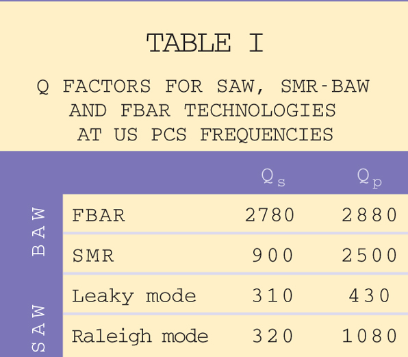
Table 1 shows a table of the Q factors for various technologies.1,2 SAW filters dominate the GSM and low frequency (< 1 GHz) space.
Cost-wise, they have the advantage of low die cost due to simple wafer processing and a large existing fully depreciated manufacturing base. SAW filters can incorporate a single-ended to differential transformation without the need for external baluns, which is a key for GSM Rx applications.
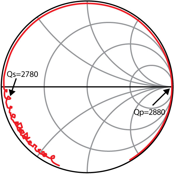
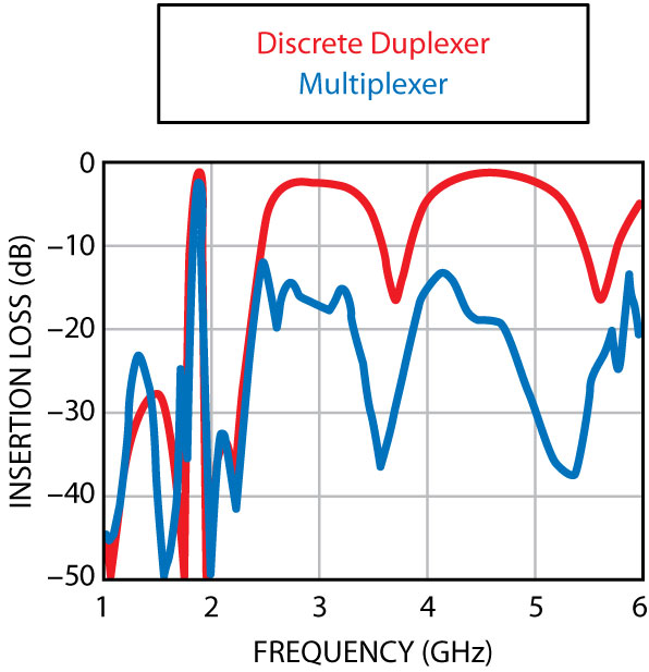
BAW technology, which comes in two flavors, FBAR and SMR, has become the standard technology for US PCS duplexer applications.12 The high Q of the FBAR filters has enabled superior insertion loss (IL) performance, especially when the bands are spaced closely together (see Figure 3).
Another of BAW’s attractive features is the potential for monolithic or above IC integration with CMOS chips, with filter/LNA/mixer SoC devices already demonstrated in the literature.1 Ceramic filters, while being very cheap and a well-established technology, are fading away due to larger size and inability to integrate.
However, having good stand-alone filters available does not necessarily guarantee good multiplexer performance. A good out-of-band return loss (RL) is needed from all the filters hooking up to the antenna as out-of-band RL is additive to the IL of each filter in the multiplexer.
FBAR technology has the best out-of-band RL (~ –0.2 dB) among the discussed filter technologies, since it uses an air interface on either side of the resonator. The air interface has a very large reflecting bandwidth while SMR-BAW and SAW both use Bragg reflectors, which have a much more limited reflecting bandwidth resulting in less attractive out-of-band (~ –0.6 dB) RL.
FBAR multiplexers have been demonstrated in phones to have 1 dB better handset sensitivity and longer battery life than designs using the same duplexers as discrete components. Up to half of the improvement is accounted for by the better out-of-band RL.
A design advantage of the multiplexer is that individual duplexers need not have excellent wideband rejection because the LC matching network provides additional wideband rejection for free. This means that the discrete duplexer performance can focus on better IL and near band rejection/isolation specs. A good example is the quintuplexer, where narrowband PCS and cell duplexers are integrated with a GPS filter.
As shown in Figure 4, a stand-alone PCS duplexer has very little out of band rejection, but the second harmonic rejection improves by more than 10 dB when incorporated in the multiplexer without any change in the duplexer design.
The Next Step
While today’s WCDMA phones are mostly single or dual-band, the future trend is towards tri-band for worldwide roaming and increased capacity within a country.
A multiplexer that utilizes the LC matching scheme should be advantageous in this application because it will allow the addition of more frequency bands without adding more switches. This is helpful because present switches already have difficulty meeting the linearity threshold needed to meet 3GPP blocking specifications without expending exceptions.
Each new switch adds more nonlinear capacitance to the module, which will increase distortion even further.
For example, tri-band configurations, such as Band 1, 2 and 5 for US-centric and Band 1, 8, (2, 4 or 5) for Europe-centric phones, could use single throw eight pole ST8P switches with a multiplexer versus adding 2 to 3 throws with a discrete duplexer solution.
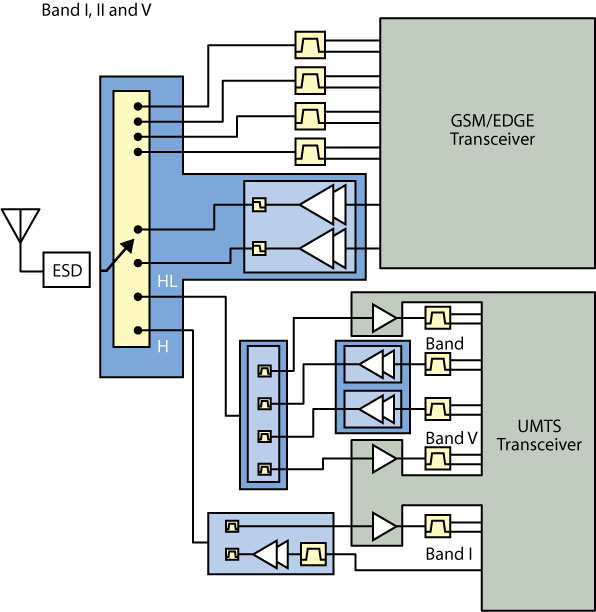
Figure 5 shows a GSM/WCDMA concept architecture with three FEMs. A Band 2, 5 multiplexer is used to reduce the number of switches needed. The switch and GSM PA are shown integrated as a FEM. The Band 1 chain is shown as an (input filter/duplexer) FEM. The savings is worthwhile, not only for size (a WCDMA switch is approximately three times the die size of a GSM Rx switch), but also in linearity. The extra wideband rejection from the LC matching network in front of the multiplexer could help to suppress certain jammer signals coming through the antenna before reaching the duplexers and thus improve IMD 2/3. Harmonics performance should also benefit from the extra out-of-band rejection suppressing the harmonics going out the other direction from the Tx chain. Eventually, it makes sense to integrate WCDMA duplexers, GSM Rx filters and the switch to make a single (switch, WCDMA, GSM) FEM even farther down the line. In this configuration, the phase angle between duplexer and switch, which has been shown to influence the amount of IMD generated in the cascaded switch/duplexer chain, can then be controlled and minimized.1
Conclusion
Multiplexers have made significant penetration in the duplexer market in recent years. The three main benefits of using multiplexers are size reduction, improved performance and speed of integration. It integrates by technology and thus can effectively leverage the expertise of filter companies. Various filter technologies and integration schemes have been presented that work in creating multiplexers with wafer level packaged filters directly attached to a single substrate as the preferred path towards even further size reduction and integration. There is a clear benefit provided by multiplexers in tri-band CDMA phones today and value in applying the same methodology in multi-band WCDMA phones in the future.
References
- F. Van Straten, B. Smolders, A. Van Zuijlen and R. Ooijman, “Multi-band Cellular RF Solutions, IEEE Journal of Solid-State Circuits, Vol. 39, No. 10, October 2004, pp. 1598–1604.
- G. Zhang, S. Chang and A. Wang, “WCDMA PCS Handset Front End Module,” 2006 IEEE MTT-S International Microwave Symposium Digest, Vol. 1, pp. 304–307.
- H. Mandai and N. Nakajima, “Passive Integration with SAW Filter Using LTCC (Low Temperature Co-fired Ceramics) and Multi-layer Technology,” 2002 IEEE Ultrasonics Symposium Proceedings, Vol. 1, pp. 81–84.
- T. Jamneala, P. Bradley, D. Feld, D. Clark and A. Chien, “A Generic Passive Matching Network for Multiplexers,” IEEE Transactions on Ultrasonics, Ferroelectrics and Frequency Control, June 2007.
- P. Bradley, J. Kim, S. Ye, B. Yu, K. Grannen, D. Lee, D. Hula and W.K. Kim, “A 6-Port Film Bulk Acoustic Resonator (FBAR) Multiplexer for US CDMA Handsets Permitting Simultaneous Use of PCS, Cellband and GPS with a Single Antenna,” 2006 IEEE Ultrasonics Symposium Proceedings.
- M. Buchsbaum, C. Korden, E. Leitgeband and H. Faulhaber, “Design of a High Integrated Triplexer Using LTCC Technology,” IEEE MTT-S International Microwave Symposium Digest, pp. 378–381.
- K. Wang, W. Mueller, R. Ruby, M. Gat, P. Bradley, A. Barfknecht, F. Geefay, C. Han, G. Gan, A. Chien and B. Ly, “High Rejection Rx Filters for GSM Handsets with Wafer Level Packaging,” 2002 IEEE Ultrasonics Symposium Proceedings, pp. 925–929.
- M. Franosch, K.G. Oppermann, A. Meckes, W. Nessler and R. Aigner, “Wafer-level Package for Bulk Acoustic Wave (BAW) Filters,” 2004 IEEE MTT-S International Microwave Symposium Digest, Vol. 2, pp. 493–496.
- H. Kando, D. Yamamoto, M. Mimura, T. Oda, A. Shimizu, K. Shimoda, E. Takata, T. Fuyutsume, R. Kubo and M. Kadota, “6B-4 RF Filter Using Boundary Acoustic Wave,” 2006 IEEE Ultrasonics Symposium Proceedings, pp. 188–191.
- M. Kadota, T. Nakao, K. Nishiyama, S. Kido, M. Kato, R. Omote, H. Yonekura, N. Takada and R. Kita, “Small SAW Duplexer for W-CDMA Full-band with Good Temperature Characteristics,” Third International Symposium on Acoustic Wave Devices for Future Mobile Communication Systems, March 2007, Chiba, Japan.
- T. Nakao, M. Kadota, K. Nishiyama, Y. Nakai, D. Yamamoto, Y. Ishiura, T. Komura, N. Takada and R. Kita, “Smaller SAW Duplexer (32.5 mm2) for US-PCS Having Good Temperature Characteristics,” Japan-Taiwan Workshop on Future Frequency Control Devices, March 2007, Chiba, Japan.
- R. Ruby, P. Bradley, Y. Oshmyansky, A. Chien and J. Larson III, “Thin Film Bulk Wave Acoustic Resonators (FBAR) for Wireless Applications,” 2001 IEEE Ultrasonics Symposium Proceedings, Vol. 1, pp. 813–821.
- K.M. Lakin “Thin Film Resonator Technology,” IEEE Transactions on Ultrasonics, Ferroelectrics and Frequency Control, Vol. 52, No. 5, May 2005, pp. 707–716.
- P. Ancey, “Above IC RF MEMS and BAW Filters: Fact or Fiction?,” Bipolar/Bi CMOS Circuits and Technology Meeting, October 2006, pp. 1–5.
- T. Ranta, J. Ella and H. Pohjonen, “Antenna Switch Linearity Requirements for GSM/WCDMA Mobile Phone Front-ends,” The European Conference on Wireless Technology, October 2005, pp. 23–26.
 Allen Chien received his BSc degree in material engineering from Catholic Polytechnic University, San Luis Obispo, CA, in 1993, and his PhD degree in materials from the University of California, Santa Barbara, CA, in 1998. He is product manager at Avago Technologies’ Wireless Semiconductor Division and is based in San Jose, CA. He has conducted research in FBAR/BAW technologies, RF MEMS and wafer level packaging.