
The extraordinary performance achievable by modern radars is delivered by a combination of advances in microwave and digital technologies, including miniaturization and increased performance of RF and microwave components, analog-to-digital and digital-to-analog converters, and the massively-parallel processing capability of Field Programmable Gate Arrays (FPGA). Much more will be required of each one to meet increasingly sophisticated threats, provide additional radar functions and operate in the increasingly electromagnetically dense signal environments of the future. This must be accomplished while reducing size, weight and power consumption (SWaP) in addition to lowering cost. This article discusses these challenges and provides insight into how the aforementioned technologies, devices and design methodologies will confront them, focusing on the receive path but also addressing the transmit path, as both must function together to provide a complete solution.
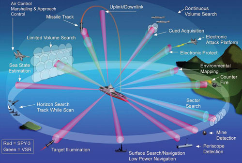
Fig. 1 Radar systems are taking on multiple functions.
The capabilities of radar systems have exploded in many directions since World War II and every year the technology absorbs more functions. Today radar systems provide not just “detection and ranging” but imaging and, most recently, some elements of electronic attack (see Figure 1). In defensive roles, radar is a highly capable adversary that is not easily fooled by the antics of Digital RF Memories (DRFM). In offensive roles, a radar system can determine in minute detail what it is “seeing” so that its operators can determine an appropriate course of action. In fire control scenarios, radars can, if so commanded, take the final step by ordering a barrage of ordinance to be directed at an approaching cruise missile as a last line of defense. Radars can function independently or within a sensor network, be aggregated to form a continents-wide network (or aperture), see through seemingly impenetrable foliage, cloud cover and structures, and function as imaging systems with graphical overlays. And this is just the short list.
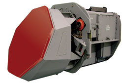
Fig. 2 Raytheon’s AN/APG-79 AESA radar for the F/A-18/E/F Super Hornet employs advanced microwave and digital components and design approaches.
Current radars are indeed impressive technological achievements but all this comes at a price – very high in the case of a large Active Electronically-Scanned Array (AESA), as shown in Figure 2. These 21st century versions of the phased-array radar are extraordinarily complex assemblages of analog, RF and microwave and digital components along with software that orchestrates system functions. Control, signal distribution and especially timing require extraordinary precision in an AESA radar that includes hundreds or thousands of antenna elements. Each of these elements potentially contains capabilities for signal capture, downconversion, format conversion, RF power generation, timing and synchronization, control, and high speed communication both within and outside the radar.
Getting the Cost Out
Not surprisingly, the Department of Defense (DoD) has mandated that the cost of future radar systems must be reduced through advancements at the device, subsystem and system levels, and with greater functional analog/digital integration, open and standardized radar architectures. Other cost-cutting strategies include use of Commercial Off the Shelf (COTS) or modified COTS components and more efficient delivery of higher RF output power in each element through solid-state devices, most likely gallium nitride (GaN) RF power transistors and MMICs. Since the first phased-array radars that combined transmit and receive functions at the element level, significant cost has been driven from the systems through elimination of the mechanical components required to steer the antenna beam.
At the highest level, the most cost reduction “for the buck” can be achieved by integrating within a single system functions, such as wide-area search, target tracking, fire control, jamming and perhaps weather monitoring, that currently require multiple systems. Networking them together with other sensors and systems allows the information the radar provides to be available in near real time over IP-based type networks to become key elements of the evolving Global Information Grid. Such multifunction systems are smaller, lighter and less power hungry and, when fully integrated, become easier for their operators to control.
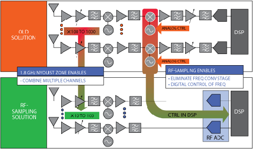
Fig. 3 The reduction in analog components is demonstrated in this diagram. (Courtesy of Texas Instruments–National Semiconductor).
The Holy Grail
The most widely held goal within DoD and prime defense contractors is to convert analog signal data to the digital domain as close to the antenna as possible. The reason is the same as for any signal processing environment, from consumer devices through radar systems: once a signal is digitized, it is vastly easier and faster to distribute, process, analyze and for its content to be modified. It also eliminates the problems associated with analog components, such as sensitivity to temperature and other environmental factors, and device tolerances. An example of this reduction is shown in Figure 3.
The device most closely associated with achieving this goal is the ADC.It is the first major signal processing component in the receive path and has the critical responsibility of passing on to the next portion of the system (typically an FPGA or FPGAs) digital representations of the original analog signal with the highest fidelity and greatest dynamic range. Using exsisting merchant market devices, it is possible to directly receive an RF input signal with an instantaneous bandwidth of DC to 6 GHz, a sampling rate of 12 Gsamples/s and 7 bits of resolution. There are a variety of devices available that reach input frequencies greater than 3 GHz with resolution beyond 12 bits. In an L-Band or S-Band radar system, use of these devices makes it possible to eliminate an entire analog downconversion stage. If the devices are operated in higher Nyquist zones it is possible to directly capture analog signals at much higher frequencies. This results in a reduction in signal-to-noise ratio, but potentially eliminates another downconversion stage.
Another technique can be used to directly digitize RF input signals at frequencies higher than an ADC can handle when operating in the first Nyquist zone, variously called bandpass sampling, harmonic sampling, IF sampling or direct IF-to-digital conversion. It allows higher IF frequencies to be employed, potentially eliminating additional analog downconversion stages and their source, mixer and filter components. The signal of interest is band-limited to a single Nyquist zone (not necessarily the first Nyquist zone), and its image will always appear in the first Nyquist zone resulting from aliasing that occurs in the sampling process. The sample rate and the desired signal band must be placed where it is isolated to a single Nyquist zone using filters, and the sample rate must be at least twice the signal bandwidth.
Mercury Computer Systems used this approach and the frequency folding that occurs during the sampling process to good advantage in a 2 to 18 GHz digital Phase Modulation on Pulse (PMOP) detector in its 2 to 18 GHz instantaneous frequency measurement (IFM) receiver. The use of digital rather than analog techniques and devices reduced the size and weight of the circuit while providing greater flexibility. A high speed, track and hold device directly digitizes the 2 to 18 GHz RF input at 1 Gsample/s. All the frequency information folds in to the first 500 MHz Nyquist zone, but phase information is preserved.
As is invariably the case in electronic design, the choice of an ADC is not so simple. This is because it is not the converter’s stated bits of resolution that is important, but rather the number of those bits that can effectively be used. The effective number of bits or ENOB is invariably less than what is stated on the device datasheet. This is a critical consideration because loss of a single bit translates into a reduction in the converter’s signal-to-noise ratio by 6 dB. In radar as well as communications and EW systems, this is a very large number. Conversely, achieving 7 effective bits from an 8-bit converter can improve radar performance in almost every respect. Spurious-free dynamic range, linearity, power consumption and other specifications ultimately determine ADC and DAC performance, and must be taken into consideration and matched with the radar system’s requirements.
Consequently, selection of an ADC for a radar application is invariably a trade-off between achieving a dynamic range of 60 dB or more that is typically required, RF input bandwidth, the number of the device’s effective bits of resolution and the Nyquist zone it can operate in without significant performance degradation. Unlike their EW counterparts, radar systems are typically concerned with processing signals of considerably narrower bandwidths, although these bandwidths have been increasing on a regular basis thanks to the use of spread spectrum modulation techniques that extend bandwidth to perhaps 1 GHz. This allows ADCs with lower RF input bandwidths and higher resolution to be used.
In a large AESA radar with perhaps 1000 elements (or more), each one with its own ADC that delivers large amounts of data to the FPGAs following it, an astonishing amount of data will be collected in a very short period of time. For example, using the aforementioned ADC with 6 GHz of RF input bandwidth, the device will be streaming about 12.5 Gbytes/s to the FPGAs following it. In only 10 s, this veritable data fire hose will have communicated 125 Gbytes of data, which the FPGA will have to ingest, process and stream further back into the system where intense computation occurs.
This amount of data is much less when bandwidths are narrower, and a radar system generally determines at an early stage what signal content is important and discards the rest. Data reduction also has a direct impact on the transmit path, as the DAC employed to reconvert the digital data to its original or modified analog form is a less onerous task.
In addition, radars are beginning to take on electronic attack roles, appearing more as DRFMs, although typically covering narrower swaths of the spectrum. Within tens of nanoseconds, they must capture the analog signals and convert them to the digital domain, store them briefly, analyze and identify them if possible from a threat library and add “techniques.” After this they must then reconvert the signal from digital to analog form, perhaps upconvert it and retransmit the signal, all within a frighteningly tiny time window, making the fidelity of the signal provided by the ADC even more critical.
Once the ADC has captured and digitized the data, the next challenge is getting it into the FPGA without incurring a bottleneck. Fortunately, as one of the FPGA’s initial functions was distributing data at high rates, the speed at which the device can do this per signal line has risen to 10 Gb/s. For those not particularly familiar with an FPGA, it consists of an array of configurable logic blocks with each cell of the block configurable (that is, programmable) to perform one of many functions. One of the most endearing attributes of the FPGA is that rather than being endowed by its manufacturer with a fixed set of functions, it is essentially a “blank canvas” when delivered to the designer, who can “paint” its desired functionality by programming it. This makes the FPGA extraordinarily versatile, as it can perform general-purpose computing, digital signal processing and high speed communication functions with little need for external resources.
The individual cells within an FPGA are interconnected by a matrix of wires and programmable switches. The logic cells become building blocks from which virtually any type of functionality can be created, from simple-state machines to complete microprocessors. The ultimate functionality that an FPGA will perform is created by programming the logic cells and selectively closing the switches in the aforementioned matrix of interconnect wires, and then combining these blocks to create the desired result.
FPGAs are extremely well suited for performing fixed-point arithmetic rather than floating-point arithmetic. Fixed-point arithmetic is typically less expensive to execute in hardware and is more efficient than its floating-point counterpart, but offers less dynamic range and requires values to be carefully scaled to avoid overflow or saturation. In contrast, in the floating-point format the position of the binary point “floats” depending on the magnitude of the number being represented. Floating-point arithmetic delivers high dynamic range and is very precise, but it comes with the caveat of being less frugal with power and more expensive to build. However, FPGAs are increasingly capable of performing both fixed and floating-point arithmetic, which further increases their usefulness in radar systems.
Although it is certainly possible to argue this point, it is a reasonable assumption that, along with the ADC, the FPGA has done more to advance the radar state-of-the-art than any other single advancement since the GaAs MMIC amplifier made solid-state T/R modules possible. Its ability to be programmed to perform a wide array of functions and its massively parallel processing make it the obvious choice for handling the increasingly vast amount of data that is sent from the ADC. Although FPGAs have integrated “soft” general processor cores, some of the latest devices have on board ARM processors that are well suited for use in the embedded computing environment of a radar system. They are also considerably easier to program than FPGAs and thanks to the widespread use of ARM processors in smartphones, there are far more engineers familiar with programming them than there are for FPGAs.
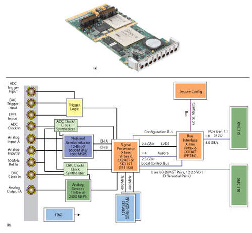
Fig. 4 The compact Mercury Computer Systems Echotek Series DCM-V6-XMC module (a) can directly digitize L-Band signals and integrates two FPGAs for signal processing and data movement and its core components (b).
FPGAs tend to follow a development path similar to Moore’s Law, with each succeeding generation delivering much greater performance. For example, the Xilinx Virtex-7, announced 18 months after the Virtex 6, provides two million logic cells, more than twice that of its predecessor, delivers up to 2.4 Terabits/s of I/O bandwidth and 4.7 TMACS of DSP performance. As touted by Xilinx in reference to radar systems, three Virtex-7 855T FPGAs can implement a 64-channel beamformer with an 80 percent reduction in board area with 24-channels per device, a 60 percent system cost reduction, and 90 percent FPGA power reduction. This type of doubling or more of performance is also typical of Altera’s Stratix devices. The result is that radar designers have come to rely on the fact that the next generation of their chosen FPGA will give them more flexibility and performance at lower power than its predecessor.
In contrast, ADCs and DACs do not generate such headline-grabbing performance increases predictably in short times. The addition of a single “effective” bit may take five to 10 years to reach the market. However, the power afforded by this single additional bit, along with reduced power consumption, a higher sampling rate and thus high RF input bandwidth, is indeed a momentous event for radar designers.
Mercury’s Echotek mezzanine module (see Figure 4) is an example of a small-form-factor module that combines a high speed digitizer and processing solution, which can directly digitize L-Band signals up to 2.7 GHz. It uses two Xilinx Virtex-6 FPGAs along with one or two 12-bit ADCs that deliver sampling rates of 3.6 Gsamples/s in a single-channel or 1.6 Gsamples/s in a dual-channel configuration. Spurious free dynamic range (SFDR) at the input is 65 dB and signal-to-noise ratio is 57.5 dB. A 14-bit, 2.5 GHz DAC provides an analog output up to 2.5 GHz with an SFDR of 50 dBc and noise spectral density of -165 dBm/Hz.
In addition to FPGAs, designers are looking closer at graphics processing units (GPU) for their ability, among other things, to deliver extremely high resolution while also being significantly easier to program than FPGAs. In addition, as the graphics engines for a broad range of consumer electronics systems, programmers with expertise in GPUs are considerably easier to find than those who can program in VHDL.
GPUs are essentially fixed-point processors with massive arrays of single- and double-precision floating point units. They provide huge processing capability, but as a result also incur significant latency because of the data pipelines required for data transfer. FPGAs allow enormous flexibility in controlling onboard infrastructure, which allows the device to be optimized to reduce latency. However, GPUs require their application to essentially be fixed in the architecture. Finally, GPUs consume significant amounts of power and are not available in a variety of sizes as are FPGAs. That said, their positive attributes are making them appealing in certain circumstances.
Microwave Technology Moves Forward
Although this article has thus far focused on the roles of ADCs, DACs and FPGAs for the advancement of radar systems, RF and microwave technology will obviously play an equally important role as radar systems evolve to face new threats. Just as GaAs MMICs broke new ground in the fabrication of T/R modules, their performance has increased and their cost has dropped dramatically, whether for small-signal applications such as low noise amplifiers, or RF power generation. Performance of both small-signal and RF power devices has improved in every important metric, from noise figure to linearity and efficiency, and in RF power devices with higher outputs at higher frequencies. All of these improvements are reflected in the capabilities of today’s radar systems, and the roadmap for GaAs as well as silicon germanium (SiGe) technology is impressive.
However, around 2005, gallium nitride (GaN) RF power transistors and later MMICs began their rise as the “next big thing” in compound semiconductors for use in RF and microwave applications. The genesis was DoD’s decision to use them for generating RF power in Improvised Explosive Device (IED) jammer amplifiers destined for Iraq and Afghanistan. Thus they were thrust from developmental to production status at an astonishing rate, even though at the time they were first employed, reliability and other benchmarks were far from proven. Nevertheless, the success of the Counter-Radio Controlled Improvised Explosive Device (RCIED) Electronic Warfare (CREW) program (now in its third generation), has made GaN a primary topic of conversation for use in other applications, one of which is radar systems.
An AESA radar can produce many sub-beams and can paint many targets over a very wide range of frequencies, but it can also concentrate all beams to produce the appearance of a single aperture. As a result, no single T/R module need deliver high RF output power, as the gain of the many antenna elements produces the desired ERP. As DoD’s goal is to increase RF power output at the element level, this makes a compelling case for broadband, high power-density, GaN-based amplifiers.
GaN’s power-added efficiency is equal to that of GaAs, but it has up to 10 times the power density (currently up to 11 W/mm of gate periphery), and a GaN-based power amplifier can deliver more than 100 W with 50 percent or greater efficiency. This supports the concept of a 1 kW CW pallet through four- or eight-way combining depending on the power level of the building block. Not too long ago, GaN’s ruggedness remained in question, but the ability to operate to a 10:1 VSWR is not unrealistic.
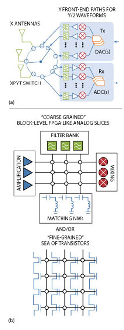
Fig. 5 The compact Mercury Computer Systems Echotek Series DCM-V6-XMC module (a) can directly digitize L-Band signals and integrates two FPGAs for signal processing and data movement and its core components (b).
However, GaN’s exceptionally high power density comes at the expense of large amounts of heat that must be dissipated both at the device, subsystem and system levels. In a radar system that has thousands of elements, each one with a GaN-powered amplifier, this is not a trivial concern. At the device level, one promising technology is the use of aluminum-diamond metal matrix composites in place of copper-moly-copper or other materials as a heat spreader.
Diamond, whether natural or synthetic, has the highest thermal conductivity of any substance, and at least twice that of its alternatives. It offers significant promise. However, it is still likely that radar, as well as EW and other systems employing high power, GaN-based amplifiers, will require some form of advanced cooling. Nevertheless, DoD is solidly behind the use of GaN, both in EW systems (of which the Next Generation Jammer is an excellent example) as well as radar systems. This virtually assures its increased use in defense applications.
Challenges for the Future
DoD has long been frustrated that it must buy multiple radars to perform similar functions rather than a single one, as there is no standardized system architecture, which results in unique, proprietary designs. That is, if five radar systems are developed by different contractors, the result will almost invariably be five different, proprietary systems that essentially serve the same mission or missions, but are different in almost every respect.
In the domain of embedded systems, standards such as VPX have made enormous strides in providing commonality between products of various vendors, and have reduced cost and perhaps increased the number of suitable products. No such situation exists in the RF and microwave domain. The entire radio interface remains almost fully proprietary, which makes it exceedingly difficult for second-tier suppliers to develop products that deliver high performance and reduce cost, significantly reducing risk.
This is perhaps one of the reasons why RF and microwave content rarely finds its way into embedded systems as have signal processing, single board computer and other functions. The RF and microwave industry, as it relates to defense systems, is famous for being a wholly custom business and there are no rules with which this technology can be integrated within standards that today are typically used for digital embedded systems. This makes clock distribution, channelization and switching in the backplane virtually impossible to integrate and there is no switchable RF systems architecture that is compatible with the bladed architecture of embedded systems. There are no constraints on RF architecture in the backplane and thus little progress in achieving greater modularity. Without an open, standardized approach it is likely that this “one-off” approach to design will continue, frustrating efforts to reduce cost.
Fortunately, there is an initiative within DoD to create open radar architectures, creating reusable “plug-and-play” subsystems and facilitating the use of COTS components from a broad array of vendors, in order to enable fast technology refresh while lowering the cost of new radar systems. There are significant benefits, including integration of legacy radar systems, easier development of multifunction radars, rapid insertion of new technology, scalable architectures, enterprise-wide sharing of information and of course, cost reduction. This is the future of defense radar systems and its necessity has become even more obvious as impending and truly draconian reductions in defense spending become more likely.
There is also, as of November 9, 2011, a broad agency announcement (BAA) from the Defense Advanced Research Projects Agency (DARPA) for what it calls an “RF-FPGA,” superficially at least an oxymoron. However, the BAA actually is, in DARPA’s words, to “enable a common hardware architecture that facilitates reutilization of the same set of RF front-end components across disparate applications through programmability of the transceiver chain. RF-FPGAs will impact the areas of communications, electronic warfare radar, and signal intelligence by eliminating redundant and costly hardware development required for the adoption or recognition of a new wireless function or waveform” – in other words, RF standardization. Hardware resulting from the program will be dynamically-programmable analog and RF blocks similar in purpose to a digital FPGA slice (see Figure 5). It aims to demonstrate working blocks of reconfigurable components and programmable transceivers capable of configuring for a variety of wireless applications while maintaining near optimal performance. Proposals are due January 26, 2012.
Conclusion
The many challenges discussed in this article are formidable, but achievable. They include producing higher levels of integration at the element level of the array, miniaturizing both digital and RF and microwave circuits, reducing power consumption, increasing resolution, delivering greater RF output power, increasing signal processing performance and ultimately converting signals from analog to digital form as close to the antenna as possible. In concert with an effort to provide a standards-based, open radar architecture and a similar effort for RF circuits, they are virtually certain to produce systems that meet the requirements of the future.
 Ian Dunn is Vice President and General Manager of Mercury Computer Systems’ Microwave & Digital Solutions Group. He was previously the company’s Chief Technology Officer responsible for technology strategy and R&D projects. Dunn joined Mercury Computer Systems in 2000 as a systems engineer upon completing his doctorate at Johns Hopkins University in Electrical Engineering. As a doctoral student there, he consulted for Disney Imagineering and Northrop Grumman on distributed automation and various high performance computing projects. Dunn has 20 years of experience designing and programming parallel computers for real-time signal processing applications and has authored many papers and a book on designing signal processing applications for high performance computer architectures.