
Product Feature
An Aluminum Nitride High Power Dissipation RF Packaging Platform
CMC Wireless Components
Phoenix, AZ
Aluminum nitride (AlN) is an ideal electrically insulating material for use in high power electronic packaging applications. Possessing both high thermal conductivity and a non-toxic chemical nature, AlN is commercially available in a wide range of package types (flanged, flangeless and arrays) for a number of different high thermal demand applications, including the housing of high power RF transistors. Because co-fired AlN is manufactured using a highly flexible, low cost soft-tooling approach, package designers are afforded tremendous flexibility in defining metallization patterns and circuit routing opportunities. This flexibility allows incorporation of both isolated and grounded devices within the same package or module.
AlN is a high melting temperature, mechanically rugged ceramic material that offers a unique combination of properties for use in high power RF packaging and has been commercially available since the early 1990s. Standard metallization systems for AlN include thin film for high resolution applications, thick film and co-fired metal compositions. All of these metallization systems are compatible with high temperature braze (above 700°C) for lead or flange attach and can be nickel and gold plated.
|
Table 1 | |
|
Material |
Thermal Conductivity |
|
LTCC |
3 to 5 |
|
Aluminum oxide, A1203 |
25 |
|
CMC high TH substrates |
200 |
|
CMC co-fired AIN |
190 to 200 |
The ability to co-fire AlN is perhaps its most unique characteristic (other co-fire systems have much lower thermal conductivity, as shown in Table 1 ). In the co-fire process, metal paste and ceramic powder consolidate at high temperature to form a fully dense ceramic/metal body (a process called sintering). This fabrication approach allows incorporation of metal layers and metal vias within the insulating ceramic body. This capability results in a dense, hermetic, high thermal conductivity substrate with "three-dimensional" wiring, yielding tremendous electrical design flexibility, thermal and electrical performance.
The recently introduced AlN High Power Dissipation Platform utilizes co-fired AlN in three different configurations: flanged, non-flanged and array format. In addition, because of the electrical design flexibility inherent in the co-fire system, each of these configurations may be produced with electrically isolated pads, grounded pads, or a mixture of isolated and grounded metallization features (vias which connect top and bottom surface metallization or pads are used to provide electrical grounding). Applications for this product platform include bipolar RF high power transistor packages (isolated versions), LDMOS RF high power transistor packages (grounded versions), multistage microwave amplifiers, multilayer image sensor packages, power circuit hybrids and laser diode submounts.
Multilayer Capability and High Thermal Conductivity
As telecommunications power levels and frequencies have increased over the past two decades, the need for ceramic packages with internal metallization layers (termed multilayer ceramic) has increased dramatically. Oxide-based co-fired ceramic systems such as low temperature co-fired ceramic (LTCC) and high temperature co-fired ceramic (HTCC) have given low power density circuits a boost in performance and reduced circuit complexity. However, as the table shows, common co-fired oxide-based packaging materials are very limited in their thermal performance.1,2
Because of the low thermal conductivity of these oxide-based, multilayer systems, these approaches "max out" at approximately 3°C/W, a power density that is barely adequate for low power driver circuitry. This clearly illustrates, for any high power application that requires a multilayer package geometry, AlN is the clear choice.
|
Table 2 | ||
|
Critical Parameter |
Traditional Ceramic |
Co-fired Aluminum Nitride |
|
Flexibility in design allowing grounded and-or isolated pads |
No |
Yes |
|
High electrical conductivity, hermetic vias for improved RF performance |
No |
Yes |
|
Available in surface-mount, leaded or array formats |
No |
Yes |
User Benefits of AlN Multilayer Technology
Critical user benefits of co-fired AlN material are summarized in Table 2 .
Traditional ceramic packages used to house bipolar transistors for the RF and microwave industry are composed of a ceramic pill (AlN, BeO or alumina) with laser-drilled vias that are metallized and then through-hole plated to provide a conducting path to ground. This pill is typically brazed to a metal flange material such as Cu/Mo/Cu (for AlN) or Cu/W (for BeO and alumina). For LDMOS devices, an alumina window frame is brazed directly to the metal flange with the device located within the window frame directly on the flange material.
|
|
|
Fig. 1 Schematic top view of ground zero package with grounded and isolated pads. |

To fabricate a co-fired, multilayer package, metallization is applied to the surface of individual ceramic layers prior to the sintering process. Vias are formed by simply punching holes in the ceramic tape and filling these holes with metal. Since vias are punched with a high speed soft-tool, the location and number of vias in each layer can easily be altered. After each individual layer is "personalized" (punched with via and surface metal patterns applied), individual layers are laminated together and then fired at high temperature to produce the final fully dense metal/ceramic composite. Internal metallization layers, such as ground or power planes, can easily be incorporated into a package design. In addition, isolated or conducting pads can be created by the presence or absence of vias connecting metallization regions to ground. This concept is illustrated in Figure 1 .
As previously mentioned, the AlN High Power Dissipation Platform consists of three different package configurations: flanged, non-flanged or array geometry. By varying soft-tool controlled via patterns, each of these configurations can be made with isolated, grounded or a mix of isolated and grounded pads to accommodate different device types. Flanged packages consist of a co-fired AlN substrate brazed to an eared or earless high thermal conductivity Cu/Mo/Cu flange. Non-flanged packages consist of a co-fired AlN substrate that can be directly surface-mounted or clamp mounted, and the array configuration consists of a matrix of co-fired AlN packages, which lend themselves to automated die assembly approaches.
Thus, the RF designer has a wide range of electrical options open to him or her, while maintaining a consistently high thermal performance: flange, surface-mount or array; isolated, grounded or a mixture of each on a single substrate. In addition, because the metal/ceramic structure is created in one high temperature operation, the resulting body has very low residual stress and is extremely rugged. This is in direct contrast, for example, with current packages manufactured by brazing thin alumina ring-frames to metal flange materials with the resultant residual stress that results from thermal expansion mismatches.
A second key advantage of the co-fire approach is the ability to produce dense, hermetic vias, which result in superior electrical grounding characteristics for the final package.
Why Are Thermal Conductivities Above Alumina Critical?
There is a broad spectrum of electronic applications that benefit from a packaging approach with high thermal performance, including motor controllers, laser diode submounts and high current switching circuits. No application, however, benefits more from enhanced thermal performance than microwave and RF transistor packages where power densities can exceed 10 kW/in2 . Any opportunity to reduce die temperatures means immediate improvements in long-term reliability - by industry standards, every 10°C temperature reduction doubles the effective device lifetime. For this type of power density, other co-fire material sets such as alumina, or LTCC, are simply not an option.
Co-fired AlN also offers some intrinsic advantages as a packaging material when compared directly to high thermal conductivity materials such as BeO and Cu/W. For example, co-fired AlN substrates brazed to Cu/Mo/Cu flanges are the same cost as BeO on Cu/W yet are non-toxic and offer improved electrical performance on a wide range of bipolar devices. For LDMOS applications, co-fired AlN packages are more mechanically robust than packages constructed with alumina ring-frames on a Cu/W flange. In addition, the AlN format can easily be manufactured in an array format that significantly lowers both the package cost and the customer's assembly costs. The AlN approach particularly lends itself to surface-mount applications where no bolthole is required.
The Critical Advantage of Dense Vias Technology
In most types of electronic packaging applications, signals from an active device must be routed between adjacent layers in the package. In the simplest case, a single layer dielectric, vias connect the top and bottom side metallization patterns. This has been accomplished in high thermal conductivity ceramic bodies, such as BeO and traditional, non-co-fired AlN, through the use of a plated-through-hole technology. Figure 2 shows a scanning electron microscope (SEM) photograph of a via plated through with gold. Note the thin layer of metal on the surface of the via.
In this approach, a hole is drilled into the dense ceramic body using a laser or an ultra-sonic cutting tool, the via walls are then metallized (thick film or thin film) followed by through-hole electroplating. Invariably, this approach results in a thinner layer of high electrical conductivity plated Au on the bottom of the via when compared to the entrance hole. This variation is due simply to geometric constraints during the electroplating process in providing efficient plating solution exchange within a cavity. This thinning of the Au layer near the bottom of the via results in a degraded ground connection within the package when compared to a solid via. A cross-section of a typical via exhibiting this phenomenon is shown in Figure 3 .
The High Power Dissipation Platform, which utilizes co-fired AlN, addresses this issue by offering solid filled vias. In this fabrication technique, a tungsten-based system is utilized for surface, interlayer and via metallization. A typical via is 0.006" in diameter (with other via sizes commonly available up to 0.020") and is filled such that the final product is fully dense, thus forming a hermetic seal. A cross-section of a typical co-fired via is shown in Figure 4 .
|
|
|
|
|
Fig. 2 Cross-sectional SEM view of a via plated through with gold. |
Fig. 3 Cross-sectional SEM view showing the thin metal layer at the bottom of the through hole via at a higher magnification. |
Fig. 4 Cross-sectional SEM view showing three dense hermetic vias in co-fired AIN structure. |


The net effect is a significantly better RF and DC electrical pathway between adjacent metallization layers in the package or between the top of the package and a ground plane or flange. This connect is so effective that these vias can be used to provide grounding for the backside of LDMOS devices, negating the necessity of bonding LDMOS devices directly to metal flanges.
|
|
|
Fig. 5 LDMOS (a) and surface-mount packages (b) constructed using co-fired AIN approach. |

The advantages of using a co-fired ceramic for LDMOS applications, particularly when a surface-mount approach is preferred, are numerous. This technology results in improved flatness and the ability to integrate the insulating ring-frame into the package during the co-fire process. This replaces the brazed on alumina frame (with its resultant residual stress) with an AlN "frame," which is simply an electrically isolated region of the co-fired package itself. This produces a mechanically rugged package for any application where surface-mounting is an option.
Also contributing to the long-term reliability of this package is the fact that lead are brazed directly onto a dense tungsten metal structure that is an integral part of the co-fired body, with lead pulls in excess of 25 lbs. This is in contrast to the typical metallization on alumina ring-frames, which depend on a Mo-Mn glassy phase for adhesion with resulting lower adhesion. An example of a co-fired AlN LDMOS package with this feature is shown in Figure 5 (flangeless configuration, grounded and isolated pads).
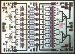
Dense hermetic vias also play a key role in improving the performance of packages designed to house bipolar devices. When the co-fired AlN approach is used, very significant improvements in device performance have been observed for a wide range of bipolar devices. A co-fired AlN bipolar package (flanged configuration, isolated pads) is shown in Figure 6 .
These performance improvements, which include significant gain improvements when directly compared to thru-via counterparts, have been attributed to the improved electrical pathway to ground provided by the company's dense, hermetic via structure.
Conclusion
|
|
|
Fig. 6 Bipolar packages constructed using co-fired AIN substrate on Cu/Mo/Cu flange. |

The AlN High Power Dissipation RF Packaging Platform has significant advantages over traditional ceramic (BeO, LTCC, HTCC) and metal flange packages. These advantages, which include excellent thermal conductivity, improved electrical performance, low cost array format options and tremendous design flexibility, dramatically open up a new range of packaging possibilities for the RF designer.
No longer constrained to either isolated or grounded package types, this approach allows the cost-effective integration of grounded or isolated pads within the same package while maintaining peak electrical and thermal performance. For more sophisticated designs, ground planes or conducting metal patterns can be incorporated within the body of the co-fired package connected with vias to appropriate surface pads. For even more demanding applications, thin film, photo-lithographically patterned metallization on one or both surfaces can be combined with co-fired thick film metal layers and/or vias below the surface.
References
1. S.J. Horowitz and D.I. Amey, presented at the 13th European Microelectronics and Packaging Conference , Strasbourg, France, May 2001.
2. For example, see NTK product data sheets for alumina co-fired packages.
CMC Wireless Components,
Phoenix, AZ
(480) 496-5027.
Circle No. 303