
TECHNICAL FEATURE
Improved Gain for a Dynamic Envelope Tracking Amplifier in Cellular Radio Handsets
An envelope tracking (ET) amplifier with variable bias voltage is a potentially more efficient power amplifier technique for third generation cellular phones. However, the input and output impedances of the transistors vary with the bias Q-point and power level. Because of the variation of impedance, the gain and efficiency of ET amplifiers decrease significantly, and the SWR and stability become worse. The mismatch of a dynamic ET amplifier cannot be substantially avoided. In this article, the use of a varactor diode to compensate this mismatch will be demonstrated. The gain improvement is experimentally shown to be 7 dB. The DC power consumption of a dynamic ET amplifier with impedance compensation is statistically 37 percent that of a fixed bias power amplifier.
In-ho Kang and Joo-yeon Kim
Korea Maritime University
Dept. of Radio Science & Engineering
Pusan, Korea
In a mobile radio transmitter with digital modulation, the RF power amplifier is required to be linear and maintain signal integrity with limited spectral regrowth. To maintain the linearity of an RF amplifier, it is usually operated in class A or class AB mode. In many wireless systems, the power transmitted by the mobile unit is adjusted such that signals arriving at a basestation from all portable transmitters have similar power levels. Because the variable distance between mobile and base units, as well as multipath and shadow fading must be accommodated, the amplifiers operate over a wide dynamic power range extending from a maximum level to 10 dB in power back-off. The probability distribution function (PDF) of the amplifier output power in a CDMA reverse link urban environment was reported by Staudinger, et al.1 Similar reports about PDF were also given by others.2,3 The operation of class A or class AB RF amplifiers below their maximum output power leads to reduced power added efficiency. The operation at the maximum output power level in mobile unit transmitters occurs for a very small fraction of the time. It is critically important to maintain efficiency at low output power levels. Hanington2 suggested an ET amplifier in which the bias voltage supplied by a DC to DC converter is a function of the power level. The efficiency of the ET amplifier can be kept high even as the output power decreases. Therefore, the ET amplifier is an efficient technique for power amplifier application in W-CDMA and cdma2000 cellular phones. The importance of ET amplifiers is expected to increase for the third and fourth generations of mobile systems. However, the input and output impedance of transistors vary with changes in the quiescent bias point (Q-point) and power level because of the variable bias of the ET amplifier. Owing to the variation of impedance, the gain and efficiency of the ET amplifier decrease considerably, and the SWR and stability become worse. In this article, the mismatch in dynamic ET amplifiers will be compensated by using varactor diodes. The improvement in gain and efficiency will be shown.
DYNAMIC ENVELOPE TRACKING AMPLIFIER WITH COMPENSATED IMPEDANCE
 |
|
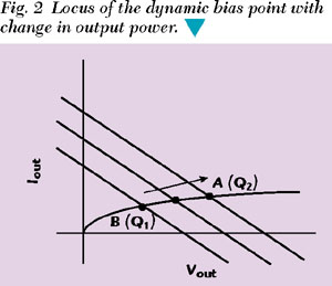
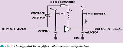
Figure 1 shows a diagram of the ET amplifier suggested by Hanington.2 The RF input signal is sampled by a directional coupler. It is then transformed into a DC signal by an envelope detector. This DC signal is so small that it cannot be directly applied to the power amplifier. Instead, it is amplified by a DC to DC converter,4 the large output of which is proportional to the input and is used to supply the dynamic bias voltage to the power amplifier. If both DC voltage and current are varied optimally, the efficiency can be kept high even as the output decreases. Figure 2 shows the locus of the dynamic bias point. The optimal bias voltage curve can be determined by the inherent tradeoff between linearity and efficiency. However, the input and output impedances of the transistor vary with the changing of power level and Q-point because of the variable bias of the ET amplifier. Because of the impedance variation, the gain and efficiency of the ET amplifier decreases significantly, and the SWR and stability become worse. If the matching network is designed for a large bias voltage and high power level, mismatching will happen at a low bias point and low power level. Hanington2 and Nishimura5 selected the matching circuit of the ET amplifier for low power and small bias voltage because the most probable output power suggested by the PDF is low. Inversely, a matching network for low power levels makes the ET amplifier mismatched at high power and large bias voltage. The decrease in efficiency at high power levels makes the requirements on the DC to DC converter more important. The conversion efficiency of the DC to DC converter is improved by using a switching type of converter. The conversion efficiency at high output DC voltages is very high, but reduced at low output power. The large output range of the DC to DC converter means that the total efficiency of the ET amplifier becomes worse at low power where the probability of need is highest. The noise characteristics of the ET amplifier become larger because of the increasing demand on the DC to DC converter. The mismatch of the ET amplifier cannot be substantially avoided over the dynamic range of output power of mobile transmitters. A varactor diode can be used as a tuning capacitance to compensate for this mismatch.6 If a reverse voltage is supplied to the varactor diode, its capacitance is changed. The varactor diodes reverse voltages, VD1 and VD2 , are varied by the output DC voltage of the envelope detector. A dynamic ET amplifier where the impedance mismatch is compensated is shown in Figure 3. The internal varactor diode capacity and area, epitaxial layer doping, and applied voltage are related by7
where
|
C(V) |
= |
capacitance of the diode at voltage V |
|
A |
= |
area of the diode |
|
N |
= |
doping level of the epitaxial layer |
|
V |
= |
reverse voltage applied to the diode |
|
Φ |
= |
built-in potential of the diode (0.6,0.8 V) |
|
n |
= |
slope of diode C-V curve |
|
K |
= |
constant |
|
|
|
|
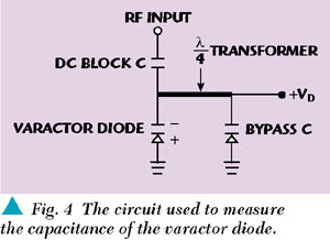
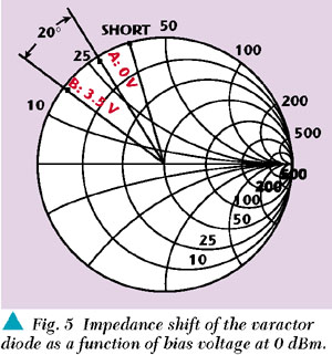
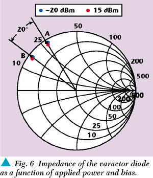
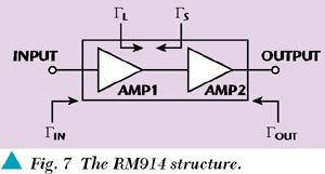
As the diode reverse bias is increased, the depletion layer increases, causing a decrease in capacitance. A 1T367 (Sony) varactor diode is used in this work. Figure 4 shows the circuit, which is used to measure the capacitance of the varactor diode. A quarter-wave transmission line is used to supply the reverse voltage. Since the varactor diode is nonlinear, 2f2 f1 frequency components in the channel band can occur and have the effect of deteriorating the characteristic of the adjacent channel power ratio (ACPR). The quarter-wave transmission line connected to the reverse bias voltage is used to prevent the distortions. The quarter-wave transmission line presents a short circuit at the even harmonics and the mixed 2f2 f1 components do not, in principle, appear. The measured capacitance of the varactor diode is shown in Figure 5. As the usual battery voltage of handsets varies from 0 to 3.5 V, the reverse voltage of the varactor diode can also be biased up to 3.5 V. In this case, a 20° phase shift is obtained for a voltage range of over 3.5 V. The short circuit point is shifted by the electrical length of the transmission line and connector. Figure 6 shows the change of capacitance as a function of the applied RF power level, which is varied from 20 to +15 dBm, for the same DC bias range. Regardless of the change in power level, the phase of the varactor diode is not varied. Experience shows, however, that the phase shift of a varactor diode occurs occasionally at high power levels. It is necessary to pay attention to the phase shifting characteristic of the varactor diode according to power level. In this work, the power amplifier module used is RM914 (Conexant Corp.). It operates in class AB for the CDMA digital modulation format. Figure 7 shows the structure of RM914. Since it is matched for a fixed bias voltage, it is mismatched at low power and low bias voltages. Inserting a varactor diode can compensate the mismatch. However, this is an RFIC circuit, composed of a two-stage amplifier. A varactor diode cannot be inserted in its interstage matching network. The input and output reflection coefficients of the circuit can be expressed as8
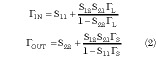
 |
 |
|
| |
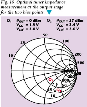
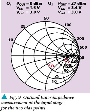
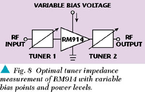
Therefore, because the mismatch of the interstage part is reflected at the input and output of the power amplifier module, the compensating matching networks composed of the varactor diodes can be connected to the input and output ports of RM914. Figure 8 shows the method used to measure the optimum input and output impedances of RM914 using tuners. At low bias voltages, tuner 1 and 2 are adjusted for the highest gain when a low RF signal is applied. They are then readjusted for highest gain when a high RF signal is applied at high bias voltages. Figure 9 shows the optimum impedance at the input stage for the different power levels and bias points. Figure 10 shows the same for the output stage. The Q1 point is the optimum impedance at the low operating point, and the Q2 point is for the high operating point. The input and output compensation matching network using the varactor diode can be designed to track the optimum impedances required. Figure 11 shows the block diagram of the ET amplifier for which the impedance variations are compensated. The layout of the varactor diode circuit can be in shunt or series or a combination shunt and series according to the trace of the optimum impedances.
|
| |
 |
 |
|
| |

RESULT AND DISCUSSION
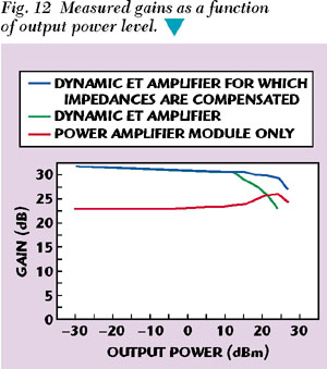
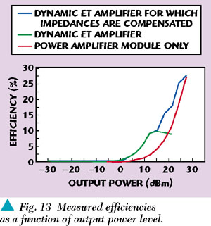
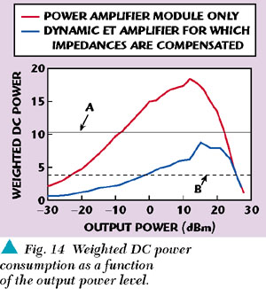
The Q1 bias point is fixed at Vcc = 1.5 V when low power is required and the Q2 bias is Vcc = 3.4 V at high power. The reverse voltages VD1 and VD2 of the varactor diodes have a range of up to 3.5 V. The reverse voltages are controlled by a DC voltage proportional to the detected voltage of the envelope detector. The Q1 bias is designed to be fixed, up to 12 dBm, with a dynamic ET amplifier. If the output power is greater than 12 dBm, the dynamic bias voltage of the ET amplifier is increased as the power increases. Figure 12 shows the gain characteristics of the power amplifier module (PAM) only, the ET amplifier and ET amplifier for which the impedances are compensated. Only in the case of the PAM does a slight mismatch occur at a respective bias and power level. The ET amplifier is designed to operate at low power levels and its gain has a tendency to decrease as the RF power level increases. The gain of the ET amplifier, for which the impedances are compensated, does not decrease as power increases. The gain improvement at high power levels is 7 dB. Figure 13 shows the efficiency curves. The efficiency of the ET amplifier for which the impedances are compensated is 2.5 times the efficiency of the ET amplifier because mismatching prevents the best possible energy transfer from one stage to the other. It means that the demand on the DC to DC converter of the ET amplifier for which the impedances are compensated will be reduced by a factor of 2.5. A DC to DC converter can be fabricated at a lower cost and the total size will be smaller. The ripple output of the switching frequency will decrease. Therefore, it is important to have the amplifier efficiency increase at the maximum output power. It is advantageous to standardize the common rules defining talk times.9 If a PDF is agreed to, it can be used to define a number of discrete weighting factors for different power levels. The DC power consumption of the dynamic ET amplifier is used at the specified power levels and weighted by the specified weighting factors given by Staudinger.1 The sum of the weighted DC power consumption is then compared to the capacity of a battery to calculate talk time. Figure 14 shows the DC power consumption multiplied by the PDF at the specified power levels. The conversion efficiency of the DC to DC converter based on Nishimura's data5 is considered in the derivation of DC power consumption. The weighted DC power consumption is high at a fixed bias voltage when the output power is 12 dBm. With reference to PDF, the operation occurs for a large fraction of the time at the 7 dBm point. The solid line A is the average power that is consumed in a fixed bias power amplifier. The dotted line B is an average weighted power that is consumed in the dynamic ET amplifier for which the impedances are compensated. The DC power consumption of a dynamic ET amplifier for which the impedances are compensated is 37 percent of the bias for a fixed power amplifier module. If the DC power consumption of a power amplifier is 60 percent of the total DC power consumption for digital modulation handsets, the lifetime of the battery is expressed as
lifetime of battery 
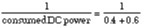
In a dynamic ET amplifier for which impedances are compensated, the factor 0.6 in the above expression is multiplied by 0.37. Therefore, the improvement in the lifetime of the battery is 1/(0.4 + 0.224) = 1.6.
Consequently, the battery lifetime of handsets is statistically increased by about 60 percent. This can play a role in decreasing the battery size of handsets. The heating effect of mobile units during calls will also be decreased because of the reduced DC power consumption.
 |
 |
|
| |
CONCLUSION
An ET amplifier with dynamic bias voltage has recently given rise to the interest of handset designers. However, the input and output impedances of an ET amplifier change when the bias point changes as a function of RF signal level. In this article, the mismatch due to dynamic bias was shown to be compensated with varactor diodes. The improvement in gain is shown experimentally to be 7 dB and the efficiency is improved considerably. The DC power consumption of the dynamic ET amplifier for which impedances are compensated is 37 percent that of a fixed bias power amplifier.
ACKNOWLEDGMENTS
The authors gratefully acknowledge O.H. Jeong and S.I. Jeong of LG Electronics, and S.U. Kim, J.T. Park and H.T. Jeong of SAMSUNG Electronics. *
References
1. J. Staudinger, B. Gilsdorf, D. Newman, G. Norris, G. Sadowniczak, R. Sherman and T. Quach, "High Efficiency CDMA RF Power Amplifier Using Dynamic Envelope Tracking Technique," 2000 IEEE MTT-S Digest, pp. 18431846.
2. G. Hanington, P. Chen, P. Asbeck and L. Lason, "High Efficiency Power Amplifier Using Dynamic Power Supply Voltage for CDMA Applications," IEEE Transactions on Microwave Theory and Techniques, Vol. 47, No. 8, August 1999, pp. 14711476.
3. J.F. Sevic, "Statistical Characterization of RF Power Amplifier Efficiency for CDMA Wireless Communication Systems," Wireless Communications Conference, Boulder, CO, August 1997, pp. 110113.
4. F. Raab and D. Rupp, "Class-S High Efficiency Amplitude Modulator," RF Design, Vol. 17. No. 5, May 1994, pp. 7074.
5. T.B. Nishimura, N. Iwata and G. Hau, "Wideband CDMA Highly Efficient Heterojunction FET Over Wide Range Output Power with DC-DC Converter," 1999 IEEE MTT-S Digest, pp. 10911094.
6. I.H. Kang, "Envelope Tracking Amplifier Having Improved Gain, Terminal for Mobile Communication Using the Same and Method for Improving Gain Relation Thereto," Patent Pending, S. Korea 10-2000-0007665.
7. U.L. Rohde and D.P. Newkirk, RF/Microwave Circuit Design for Wireless Application, Wiley-Interscience, 2000, pp. 155156.
8. G. Gonzalez, Microwave Transistor Amplifiers Analysis and Design, Second Edition, Prentice Hall, 1997, pp. 213214.
9. H. Lilja and H. Mattila, "WCDMA Power Amplifier Requirements and Efficiency Optimization Criteria," 1999 IEEE MTT-S Digest, pp. 18431846.
|
In-ho Kang received his BS, MS and DS degrees from Sogang University in 1986, 1989 and 1995, respectively. Joo-yeon Kim received his BS and MS degrees in radio science & engineering from Korea Maritime University, Pusan, Korea. |