
LTE systems are uplink limited. While base station radios generally transmit at 60 W or higher for the downlink, a handset is currently limited to Power Class 3, which allows maximum transmitter power of +23 dBm ±2 dB at the antenna port. With similar propagation characteristics for downlink and uplink, the effective throughput for uplink LTE can be much lower than for the downlink. This is especially problematic at the higher frequency bands (e.g., 2.5 GHz), where the downlink can penetrate the wall of a building, but the uplink signal is about 6 dB weaker, and the two-way connection is lost. In LTE, the uplink is not optional, since the system needs a continuous uplink for channel estimation and power control. So uplink issues are simply perceived as poor coverage.
For TD-LTE, the time spent in uplink mode reduces the time available for downlink. This means that an inefficient uplink can reduce the capacity in the system for downlink traffic. The large TD-LTE operators, including Sprint and China Mobile, have pushed standards that support higher uplink transmitter power. Handsets with Power Class 2 operation should reach the market during the next year, with output power in Band 41 (i.e., 2.5 GHz) of +26 dBm ±2 dB. This is known as high power user equipment (HPUE) operation.
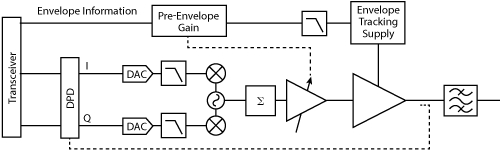
Figure 1 Simplified block diagram of ET in a handset transmitter.
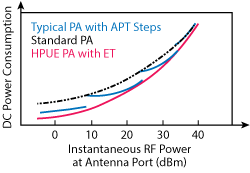
Figure 2 Instantaneous efficiency of three PA architectures.
In today’s mobile handset designs, targeting +26 dBm at the antenna port requires the power amplifier (PA) to have an output in the range of +30 to +32 dBm. Handsets with 15 or more bands have complex plumbing in the front end, with switches and filters between the PA and the antenna that contribute between 4 and 6 dB of loss. Adding HPUE operation requires the PA supporting the handset’s high band transmitter to be redesigned. Doubling the output power typically results in a much larger amplifier; however, during most operating conditions the efficiency will be lower than before, and more heat will be dissipated. It’s a waste of battery power to simply scale up the PA. Traditional amplifier designs have adopted average power tracking (APT), where the power supply is set to a static voltage based on the average RF power level. In many cases, sections of the PA can be switched in or out of the circuit, allowing the use of a smaller amplifier at lower power levels to improve efficiency. APT typically improves efficiency compared to a simple PA.
Envelope tracking (ET) is an alternative to increase the output power of the amplifier. ET requires dynamic scaling of the power supply voltage to the amplifier (see Figure 1). As the waveform ramps up for high peaks in the signal, the power supply provides the PA with higher supply voltage. In future HPUE implementations, the power supply will boost the supply voltage higher than the 3.5 V battery voltage in the handset. As the bias voltage changes, the operating point of the PA tracks to operate at its highest efficiency. When implemented properly, this approach results in the best possible efficiency at every operating point, with longer battery life and less heat dissipation in the handset. Figure 2 compares the efficiency of the three PA architectures.
ET DESIGN CHALLENGES
Digital predistortion (DPD) is an important part of making ET work. As ET technology has developed over the past 20 years, designers have found that semiconductors exhibit “memory effects,” where the device’s distortion depends on the RF power during the previous 10 to 20 ns. Essentially, the instantaneous temperature in the device channel impacts the distortion. To compensate, DPD takes recent power levels into account, applying a tailored cancellation signal to offset intermodulation distortion. DPD can improve efficiency by allowing the designer to choose a smaller PA and run it further into compression during signal peaks, because the DPD compensates.

Figure 3 APT vs. ET PA efficiency with a high PAR waveform.
ET generates out-of-band noise, due to the imperfect performance of the wideband modulator applied to the power supply. Close integration of the ET PA with a filter is important to eliminate these spurious emissions without losing efficiency. While Figure 1 shows the filter as a separate component, it’s important to co-design the filter with the PA. Matching each component to 50 Ω would greatly reduce efficiency.
The ET approach requires tight coordination between the modem chipset, power supply IC and amplifier. These three components must be carefully aligned to control the gain and time delay between the power supply voltage and the RF waveform. Precise calibration of the delay in production is critical to producing hundreds of millions of handsets. Achieving such tight control requires give-and-take between the transceiver, PA and power supply vendors. For this reason, the leading ET solutions come from chipset companies that supply all three functions.
Boosting a small amplifier to higher output power avoids scaling to a larger, less efficient PA. An ET system boosts the power supply to higher bias voltages—higher than the nominal 3.5 V of a handset battery using the right power supply components—which increases the operating point of the PA beyond its previous limits without sacrificing efficiency. APT amplifiers can also boost the power by supporting higher bias voltages. However, an APT implementation is less efficient for high power LTE, because the constant fluctuation of power in a high peak-to-average waveform results in significant time spent under inefficient operating conditions (see Figure 3). Also, ET will be easier for many OEMs to accept than APT: with an ET solution, the modified power supply is provided by the same vendor as the transceiver. In the APT case, an additional power supply device must be added to the handset, taking up board space and adding cost.
MANUFACTURING CHALLENGES
ET manufacturing has proven to be as challenging as the basic technology. Introducing ET to high volume handset production during the past two years revealed problems calibrating the time delay and gain settings. One requirement is calibrating the delay in the RF path and the timing of the power supply envelope. In the early development of ET, with signal bandwidth of 1.25 MHz, delay was not critical; more than 10 ns was acceptable. With a 20 MHz LTE signal, the delay mismatch over all operating conditions must be below about 2 ns. Next year, when 40 MHz LTE channels implement ET, delay mismatch must be less than 1 ns. Production testing has evolved to tackle this challenge, with additional hooks built into the transceiver so the transceiver receives feedback on the delay mismatch and can automatically minimize it.

Figure 4 Galaxy S7 smartphone.
Gain over temperature has also been a production headache. A handset OEM typically characterizes about 10 handset models over 10 to 15 frequency bands and some 10 temperatures. The OEM then creates a lookup table to adjust PA gain over temperature. This tedious task can cost at least $100,000 for test chambers, equipment and technician support. For an OEM that makes 200 million handsets, this cost—$0.0005 per handset —is trivial. However, for an OEM that manufactures only one million handsets of each design, the cost is $0.10 per handset. To address this, DPD introduces a feedback path to sense the output signal, and this information can be used to reduce the cost and hassle of testing. When implemented, characterization testing can be reduced to just a single test at room temperature.
The benefits of ET have been realized in most recent premium handset models, including the Samsung Galaxy S7 (see Figure 4), the Xiaomi Mi5 and many others. Calibration and characterization are still expensive in these production models, but it’s clear that high volume experience will lead to cost savings and process simplification over time. New ET devices in flagship smartphone platforms are already making significant strides to streamline manufacturing.
CONCLUSION
As video chat and augmented reality (AR) applications rise in popularity, uplink data capacity will become more important. Today, Band 41 operators are pushing for HPUE operation; in a few years, higher power operation will be required in all TDD bands, as well as high frequency FDD bands without legacy 2G/3G/4G technology, such as Band 7 (i.e., 2.5 GHz uplink). No smartphone OEM wants to add another power supply to boost voltage, and nobody wants to waste battery power. ET should become commonplace in mid-tier handsets as well as premium platforms over the next two years.