
The New World of Communications Design Software
Ansoft Corp.
Pittsburgh, PA
|
|
The world of wired and wireless communications is undergoing fervent change. Ten years ago, cell phones were bulky and expensive, and GaAs and MMICS were the technology of choice for RF and microwave applications. Today, cell phones fit in shirt pockets, and Si and SiGe are more cost-effective in the RF/microwave region. Ten years from now, projections indicate that cell phones will carry video as well as sound, low cost, high volume digital and analog technology will replace current devices, and most electronic devices will be Bluetooth enabled. Clearly design challenges are greater today than at any time in the past.
To meet this explosive demand, design groups struggle to reduce time to market. Time-consuming multiple design iterations are still the norm. The need for redesign is often due to poorly modeled phenomena and/or a lack of analysis capability for communications applications. Removing uncertainty early in the design flow is as critical to productivity as design automation itself. A new world of communications design software is required to meet the demands of this changing landscape. In this world, correct designs are produced by modeling all physical and software aspects of communications, and by seamless integration of expanded communication analyses with design and manufacturing requirements.
ANSOFT DESIGNER
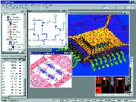
Ansoft Designer is the first entry into this new world of communications design software, introducing advanced modeling and wireless simulation with "solver on demand" technology and "environment-based" layout. The "what you see is what you get" modeling, simulation and manufacturing capability of Ansoft Designer eliminates risk by providing engineers with the information necessary to make correct decisions during the critical stages of the design process. Complex wireless design is addressed thoroughly by integrating digital communication system and wireless-nonlinear circuit simulation with powerful electromagnetic analysis, as shown in Figure 1. Multiple solver technology and advanced integration allows users to employ the appropriate modeling and simulation tool for the device under consideration.
The all-new interface makes design tasks easier and less prone to user error. The new layout editor contains advanced concepts that enable designers to work in both MMIC and RFIC environments, as well as PCB and multi-chip module (MCM) environments with equal ease. To ensure that the simulated electrical models represent the actual physical structure, the feature-rich layout editor facilitates physical design for both simulation and manufacturing. Losses computed in electromagnetic and circuit simulation can be imported into three-dimensional thermal simulation to determine the heating and temperature distribution in system components.
Ansoft Designer incorporates design automation features employing the latest Windows technology. Flexibility and customization are built in to address the needs of both the casual and power user. The design suite offers many innovations to standard design processes, which minimize effort and potential user error without sacrificing power and functionality.
NEW LEVELS OF INTEGRATION
The product integration in Ansoft Designer goes beyond a shared interface and co-simulation. Based on an all-new object-oriented architecture, the environment introduces advanced integration features such as "solver on demand" and "drag and drop subcircuit icons." Solver on demand lets users employ the best simulation technology for every design problem. Traces may be simulated by Serenade's physics-based models or directly by multiple electromagnetic solvers. Extending the use of solver-based subcircuits, "drag and drop subcircuit icons" let users build up networks with subcircuits defined in the project tree.
By maintaining a transparent separation of the desktop, editors and analysis products, the new software architecture lets users access various components on remote machines. Simultaneous access to simulators and data greatly enhanced team productivity by eliminating downtime. Design efforts can continue while lengthier simulations are performed elsewhere and are embedded back into the overall project automatically upon completion. By promoting flexibility, speed and information re-use, designers are encouraged to fully investigate overall behavior before committing a design to fabrication.
Integration in Ansoft Designer automates the process of distributing information to various simulators and assembling the results. Designers are able to create parameterized subcircuits at all levels of design for use in larger circuits. For instance, a system project may contain circuit components that will be analyzed or optimized with the nonlinear circuit simulator Serenade,® the method of moments planar simulator Ensemble,® the three-dimensional finite element simulator HFSS or the three-dimensional parasitic extraction tool SPICElink. System designers are able to choose between rapid simulation with behavioral models, more detailed harmonic balance simulation, or even more detailed electromagnetic analysis.
ADVANCED MODELING CAPABILITY
Package and board electromagnetic effects often distort real world components from ideal 50- systems. In the past, the desired performance may have been achieved by tweaking the response with off-chip board components. However, as the component count for an average mobile phone drops from approximately 200 discrete parts today to the projected 50 for the year 2004, this approach will no longer be viable. Additionally, reduced part counts require integrating more functionality within a given package (for example, SoC or SiP) leading to greater component coupling. Both situations are addressed by new advanced modeling capabilities.
|
|
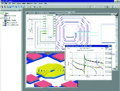
Ansoft Designer employs the finite element simulation tool Ansoft HFSS for three-dimensional electromagnetic simulation and the method of moments tool Ensemble for planar simulation. Full-Wave Spice is a new technology that provides efficient, analytical transformations between the electromagnetic and circuit levels. Full-Wave Spice uses reduced-order models of the dominant poles and zeros of the electromagnetic system to provide broadband fast frequency sweeps and rapid, detailed transient waveforms at the circuit level. Figure 2 shows a Full-Wave Spice model extraction of a stacked spiral inductor.
For electrically short structures, engineers can opt to use very fast quasi-static extraction techniques found in SPICElink and TPA (Turbo Package Analyzer).
NEW CAPABILITIES TARGET WIRELESS NEEDS
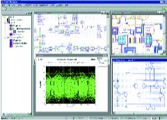
Wireless systems deliver capacity and security by mixing signal processing with RF components that perform over widely varying operating conditions. Ansoft Designer includes a dedicated end-to-end communication system simulator, Symphony. Symphony provides time-domain, frequency-domain and mixed-mode analysis for arbitrary system topologies, and simulates performance metrics such as bit error rate, error vector magnitude, adjacent channel power ratio, signal to noise and distortion, and peak-to-average power ratio. While continually evolving standard specifications have made it difficult for electronic design automation (EDA) vendors to provide up-to-date 3G libraries, both Serenade and Symphony support current bit accurate, user-configurable 3G waveforms, including W-CDMA, CDMA2000, TD-SCDMA and HIPERLAN/2. Figure 3 shows the W-CDMA standard applied to an RFIC simulation.
Another exciting development is the new transient analysis and circuit envelope solvers that have been added to the existing harmonic balance engine. The new time-domain transient analysis lets designers simulate components such as VCOs and amplifiers during power-up, RF and DC switching, or non-sinusoidal excitation.
The transient analysis features an embedded convolution engine to address frequency-domain linear models or S-parameter data files in the circuit. Either Serenade's harmonic balance or transient analysis may be applied to the same circuit without additional set-up.
Using time-sequenced harmonic balance to analyze arbitrarily modulated RF waveforms, the new circuit envelope engine is well suited for wideband or multi-carrier amplifier simulation, as well as pulsed RF-carrier analysis. This capability compliments the powerful Fast ACPR and Fast ACPR optimization capability that was introduced several years ago in Serenade.
Serenade now offers load and source pull analysis. The analysis yields contour data plots and is ideal for determining the proper termination for amplifiers, mixers or oscillators. Additionally, interpretive user-defined models (UDM) are now available. Users may define the current-voltage, charge-voltage and noise equations of a generic component. Interpretive UDMs are created directly in the schematic without the need to write and compile code. This feature allows rapid development and verification of device models.
|
|
NEW INTEGRATED IC AND PCB LAYOUT EDITOR
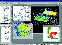
The object-oriented programming used by the Ansoft Designer automatically connects electrical and physical models, vastly simplifying the design process for engineers. Components may be represented as an electrical symbol in the schematic editor or as a layout cell (or symbol) in the fully integrated layout editor. Component parameters may be edited from either view. Also, electrical elements without physical representation, such as RF ports, may be placed directly in the layout. Now, circuits can be built, simulated and tuned (or optimized) directly from layout. Figure 4 shows the transient analysis of a multilayer PCB.
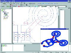
The layout editor contains a full set of primitives and functions (for example, union, subtract). Users can create IC cells or footprints. Layout elements can be edited interactively via keyboard or through the graphical user interface (select drag, stretch, move or rotate). Components created from the editor or imported from GDSII or DXF files may be macro-based (Java Script or Visual Basic) for parameterized cell or footprint development. The environment includes a powerful 3D viewer that allows the user to rotate objects and selectively hide layers for better viewing of complex multi-layer structures. Figure 5 shows the analysis of an LC tank circuit for a Bluetooth VCO.
Ansoft Designer features user-defined stationary so that component libraries and material properties can be customized to a desired manufacturing process. Information specific to the medium is pre-set based on stationary choice. The stationary may be set to a supported IC foundry or PCB process and the material property information and device libraries will default to those associated with that stationary. This feature saves the designer valuable time, labor and potential error from parameter entry, material definitions and component searching. Subcircuits based on different stationary may be combined at the project level or through hierarchy.
DESIGN FLOW AND FOUNDRY SUPPORT
EDA today connects the designer to the electrical and physical details of elements associated with a given manufacturing process through automation. Component behavior and physical attributes are obtained through device model libraries, typically created by the foundry for use with specific design tools. To provide users with access to foundry-specific device model libraries, Ansoft and several GaAs, Si and SiGe foundries are currently implementing design kits specifically for Ansoft Designer. These foundry design kits will be available with the release of the new environment. For flexible support of common design flows, Ansoft Designer also offers AnsoftLinks for interfacing to third party layout tools from Mentor, Cadence and Zuken.
ANSOFT DESIGNER FEATURES
Highlighted features of Ansoft Designer include:
· digital communication system simulation with up-to-date 3G (W-CDMA, CDMA2000, TD-SCDMA) sources
· nonlinear circuit simulation, including harmonic balance, transient analysis and modulation-based harmonic balance (circuit envelope)
· SVD FastSolve method-of-moments planar solver with lossy semiconductor analysis and Full-Wave Spice
· 3D electromagnetic field solver and parasitic extraction including Full-Wave Spice
· Integrated IC and PCB layout editor with automatic linkage between layout/schematic components
· multiple projects within the environment, multi-page schematics, all project(s) information contained in a single file for better archiving
· Arbitrary parameters may now be defined as swept values. This allows circuit performance related to component values. For example, the output frequency of an oscillator may be examined as a function of a component parameter value used as a resonator
· Support of parameterized subcircuits and parameter scoping (local, parent, global) allows the creation and use of process specific models (equivalent circuits). Electrical model parameters may be linked to physical attributes and scaled per user definition
· The optimization utility is now greatly expanded to allow more functionality and easier implementation of goals. The new utility allows optimization to user-defined equations, simultaneous optimization of behavior relative to different analyses (linear, nonlinear, transient) and an equation calculator for creating optimization goals
· Real-time tuning with slide control and auto-plot refresh has been added
· Advanced user interface
Ansoft Corp.,
Pittsburgh, PA (412) 261-3200.
Circle No. 301