CMOS technology continues to gain market acceptance for high performance applications due to the combination of low cost, high level integration and availability. As a result, more engineers are experimenting with CMOS processes and customizing new methodologies to integrate RF, analog and digital circuits in a single chip. The ability to integrate more functionality in CMOS leads to larger transistor counts and more complex circuit topologies. These larger, mixed-signal circuits can cause traditional simulators to experience convergence failures and/or reach practical limitations based on simulation speed. Design success is further complicated by the need to accurately characterize critical on-chip passive components fabricated on lossy semiconductor substrates operating at higher frequencies. Therefore, new simulation tools and methodologies must be adapted in order to successfully implement RF designs in CMOS for today’s wireless standards. This article examines these challenges as applied to high performance CMOS RFICs, specifically addressing electrical modeling, circuit simulation and specific design flow requirements.
Passive Component Modeling and Synthesis Challenges
Given the lossy nature of the silicon substrates used in CMOS processes, a sizable engineering effort is focused on reducing the substrate coupling which causes poor electrical performance. Due to their relatively large substrate area, on-chip inductors are particularly prone to substrate coupling. Inductor reactance and Q are critical in establishing the overall performance of low noise amplifiers, oscillators and other impedance-tuned circuits. By reducing substrate coupling, higher Q inductors can be obtained. Substrate coupling is reduced through a variety of novel structures and processing techniques, including pattern ground shields, deep trenches,
and suspended and vertical trace metal construction. In addition to these various structure types, inductor performance is also determined by line width, spacing, outer radius, number of turns, shape (square, hexagonal, octagonal, circular...), metal layer material, etc. The potential number of geometric variations is too large to implement a component model library database practically through fabrication and measurement-based characterization. The lack of accurate and scalable models for on-chip spiral inductors presents a challenging problem for RFIC designers. Fortunately, 3D electromagnetic (EM) simulation provides a proven method for characterizing any arbitrarily shaped on- or off-chip structures.
Ansoft’s full-wave 3D EM simulator, HFSS, was used to characterize a series of square spiral inductors that had been fabricated for use as test patterns. The inductor shape, outer diameter, line width and spacing were held fixed while the number of turns was varied from 1.5 to 5.5 turns, in one-turn increments. To reduce the amount of engineering time required to draw these inductor variations, it is common practice to develop a parameterized component footprint or P-cell using the layout tool of choice and the appropriate scripting language. Three independent methods were employed for generating a parameterized HFSS inductor in order to demonstrate design flow flexibility.

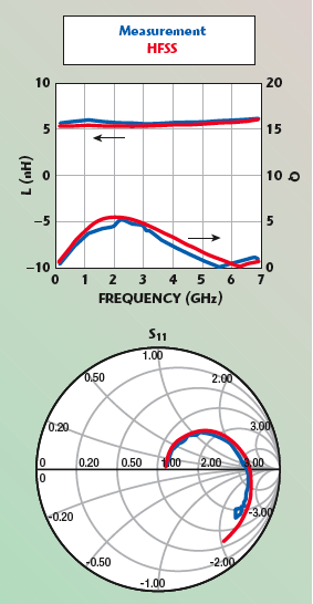
The first approach implemented the structure directly in HFSS using the 3D modeler, parameterization of geometric properties and user-defined primitives. The HFSS parameterized inductor was then used to generate S-parameters imported back into the circuit simulator of choice. With this approach the EM simulator and layout structures are independent and the user must work to ensure faithful representation. The second method applied Ansoft Designer’s footprint editor and scripting capability to create a parameterized layout structure and stack-up that could be automatically exported into an extruded 3D HFSS object. The parameterized HFSS structure can then be dynamically linked back into the circuit simulation, saving manual effort. The third approach used Ansoft Designer to import a GDSII file from a single instance of P-cell that was generated using the Cadence Virtuoso IC layout tool along with the corresponding layer map file containing the stack-up information. Ansoft Designer then exported the extruded structure into HFSS and the resulting S-parameters were used in the circuit simulator of choice. This approach takes advantage of existing design tools and scripted P-cells but is generally more manually intensive, especially when numerous parametric permutations are to be applied. Figure 1 shows the spiral inductor test patterns, which include the inductor, a ground ring and wafer probe launch pad. The values of inductance and Q are plotted as a function of frequency and number of turns. As the number of turns increases so does the substrate coupling, leading to a decrease in the value of maximum Q. The simulation also shows the inductance value increasing with the number of turns except at higher frequencies where a parasitic capacitance begins to dominate the structure’s overall reactance. Much of this parasitic behavior is related to the capacitive coupling between the ground ring and the actual inductor. Since the ground ring is only present for performing measurements with test probes and would not be present in the actual circuit, it is advisable to characterize the ground ring separately and de-embed its behavior from the measured results. When comparing EM simulation to measurements, it is imperative that the measured and simulated structures are faithfully replicated. Therefore, the effect of the ground ring must be removed from both the measured and simulated results. This is accomplished by using an Ansoft Designer schematic to de-embed the S-parameters obtained for the open-circuited ground ring from those obtained for the entire structure. After de-embedding the effects of the ground ring on the spiral inductance, the measured versus EM simulated results for inductance, Q and impedance of a 3.5 turn spiral shows excellent agreement, as shown in Figure 2. The agreement between the measurement and EM simulation validates the representation of the CMOS physical structure in HFSS and allows the engineer to perform additional electrical modeling for any geometric variation without the need for physical prototyping. In fact, the reliability, efficiency and cost savings of EM simulation in RF, microwave and high speed design over a manufacture and test approach has led to its widespread adoption. Recent design automation, exemplified by the implementation of an EM-based design flow, specifically addresses the need for scalable passive models. EM simulation combined with parameterization and distributed computation of parametric analysis helps design teams generate a practical IC passive component library quickly and efficiently. Alternatively, engineers can modify and characterize passive components “on-the-fly” via dynamic co-simulation. With the resulting electrical models incorporated into the circuit simulation via dynamic co-simulation, designers can parametrically “tweak” components for more flexible and accurate “what if” analyses of the overall design.

On-chip Component Coupling
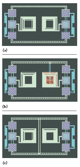
The next consideration for RF design on CMOS involves the electromagnetic coupling (or isolation) between basic structures, namely metal pads, traces and spiral inductors implemented with a CMOS process. Electromagnetic simulation was again used to characterize the IC performance and to develop design guidelines regarding minimum passive component spacing in order to avoid proximity effects. Through EM analysis, the isolation characteristics of guard rings and pattern ground shield (PGS) layers for cross-talk suppression between RF blocks was investigated. This particular study examined the coupling between two planar spiral inductors when no isolating structure was used (a) and when either a PGS layer (b) or ground guide (c) isolation design was employed. The layout of the test patterns for the three cases is shown in Figure 3.
Field visualization of the structure in HFSS reveals how the E and H fields couple (at a sample frequency of 5 GHz) inside the silicon dioxide layer and the silicon substrate layer. From the field intensity plots, one quickly recognizes that the ground guide isolation has a profound effect on reducing the energy that is coupled from one inductor to a neighboring one, as shown in Figure 4. Comparing the S-parameters from the three different configurations confirms the improved isolation offered by the ground guide (outside of the 6.75 GHz resonance observed with the non-isolated and PGS layer structures). A designer’s guide would use this information to target improved isolation between passive components and recommend the inclusion of a grounded guide or minimum component spacing. Again, measurements of the ground guided inductor pair shows excellent agreement with the EM simulation, as shown in Figure 5.
High Performance RF Design in CMOS

At this point, further tool requirements for RF design in CMOS are examined with a specific circuit block example. The architectures employed in today’s communication systems often require sources with fast settling times and low phase noise in order to provide the agile, high quality signal fidelity called for by the latest wireless standards. These RF sources are being addressed by a new generation of frequency synthesizers. At the heart of these frequency synthesizers and phase-locked loops is a voltage-controlled oscillator (VCO). Implementing a VCO in CMOS allows a single chip solution and the potential to save millions of dollars during large-scale production. New simulation, modeling and design automation technologies are utilized in the following CMOS-based VCO. The VCO will be fabricated with a standard 0.25 μm CMOS process. A circuit schematic for a single MOSFET biasing circuit is created in order to determine the I-V characteristics of the transistors that will be used in this design (see Figure 6). The actual VCO circuit topology is shown in the schematic of Figure 7. Note that in this phase of the design, the circuit is represented only by foundry models for the RF-MOSFETS as well as ideal models for the MIM capacitors, spiral inductors and thin-film resistors. Components are connected with ideal “wires,” initially disregarding the contribution of interconnecting trace metals (transmission lines) on circuit behavior. The “ideal” circuit will guide engineering decisions concerning proper device scaling, biasing and tuning for the desired output frequency, phase noise and other key performance metrics. Prior to fabrication, it will be critical to replace the ideal models with the more accurate EM-based models and make the fine adjustments to the circuit design that are needed to compensate for performance shifts attributed to device parasitics. Several key results from the preliminary design are shown in the figure. Using the Nexxim circuit simulator from Ansoft, the spectral response of the VCO can be simulated and plotted, capturing the output frequency and power level at four different tuning voltages, the steady-state voltage-wave output as well as the transient start-up behavior. Nexxim’s harmonic balance simulator provides a faster, more efficient broad spectrum analysis of spurious harmonic output than is possible with a traditional time domain or periodic steady-state (PSS) simulation, which would have to sample fine time steps over a long period in order to capture the full-spectral response. With the initial design providing the desired performance, the ideal components are replaced with their EM counterparts and the circuit layout is performed. Several tool choices are available to the design team when it comes to generating the layout. Considerations include tool availability and the existence of a foundry process design kit (PDK) including component P-cells. This particular design was implemented in the Cadence Virtuoso IC layout editor as well as in the Ansoft Designer layout editor (see Figure 8), the former providing an advantage when subsequent EM co-simulation is required for design verification. It is recognized that the spiral inductors in the LC-tank circuitry will have a sizable impact on performance; therefore, the performance shift due to the inductor behavior is first examined. Several different methods for incorporating the spiral model data into the circuit are available to the designer. While the HFSS generated spiral inductor model could be imported into any circuit simulator which supports S-parameters or Ansoft’s Full-wave SPICE model, this example took advantage of the dynamic co-simulation between HFSS and Nexxim. The full-parameterized HFSS project containing the spiral was inserted into the Ansoft Designer schematic (see Figure 9) and Nexxim was used to simulate the shifted performance, as shown in Figure 10. The two 1.5-turn inductors led to a 200 MHz shift in oscillation frequency.

Design Verification and Measured Results
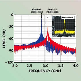
Verification of the entire IC requires the simulation of all critical performance metrics, operating conditions and process variations using a circuit model that includes all critical parasitics. For this final stage of analysis, Nexxim, Ansoft Designer and HFSS were used together to perform swept parametric time and frequency domain analyses. Integration between these three tools allows the entire passive portion of the VCO layout to be characterized by HFSS and embedded into the Nexxim nonlinear circuit simulation (see Figure 11). The non-negligible parasitics of the IC package were also investigated and included as part of the circuit model. With a fully verified circuit performing as required, the design was fabricated and tested. Through precise modeling of the passive on-chip components and interconnects, excellent correlation between the simulated and measured results was achieved. The inclusion of the HFSS-based spiral inductor led to a considerable shift in the simulated oscillation frequency. The new simulated value of –11.49 dBm output power at 3.0975 GHz was virtually identical to the measured result of –12.15 dBm at 3.094 GHz, as shown in Figure 12. The harmonic balance oscillator analysis in Nexxim accurately simulated the output spectrum of this autonomous-source circuit, faithfully capturing the harmonically-related spurious output tones up to the measurement range limit of 26.5 GHz (see Figure 13). The measured versus simulated phase noise results are shown in Figure 14. The simulated result showed a phase noise of –99 dBc/Hz at a 3 MHz carrier offset. The measured result showed good correlation with a phase noise of –100.7 dBc/Hz at a 3 MHz carrier offset.

Conclusion
The economical advantages of implementing wireless designs in CMOS are evident by the number of electronic RF devices targeting this process. The lossy nature of the silicon substrate dictates the use of novel IC structures to minimize substrate coupling as well as the use of new analysis tools to capture the uncertain electrical behavior of these new structures. It is also imperative to simulate all critical performance metrics by which the commercial product is specified. This calls for parametric analyses in the time and frequency domains. These extraction and circuit simulation technologies must be coupled to a design flow that facilitates schematic and layout editing with parameterized layout cells (preferably organized into a process design kit) for manufacturing as well as to an EM simulator that will make the simulation results more reliable. Advances in EM modeling, circuit simulation and design flow automation are making first-pass design success possible, as is evident by the correlation between measured and simulated results in the example presented.