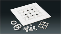
At a recent tradeshow, our two associated brands, Laser Services and Accumet, were discussing the unique substrate and material processing requirements of the RF and microwave and medical industries with a group of supply chain managers. What we continue to hear is that without smaller stocking distributors of Kyocera, Coorstek, and Ceramtech ceramic substrates like us, who offer a full suite of processing and machining services, a critical component in these microelectronics manufacturers’ supply chains would be missing. While they may maintain some higher volume/bulk buys of non-processed ceramics, etc. with larger distributors, value-added processing centers and job shops like us are where they can find their low volume, and quick-turn prototyping when they don’t know where to turn or how to get things processed for fast delivery. So by stocking popular materials like alumina, aluminum nitride, beryllium oxide (BeO), tungsten carbide, fused silica and more, they can count on us like their own personal stockroom to deliver just-in-time—and fully processed!
We stock ceramic substrates, metals, foils, epoxies, microwave absorbers, 3M medical adhesives, plastics, frozen epoxies, Kevlar, Teflon, and whatever other materials designers and procurement agents are looking for in a pinch. When they want them to come fully cut, drilled, welded, scribed, etched or marked, we are the processing partner who stocks these materials and becomes an invaluable resource. While name brand suppliers and large distributors are often the first source of supply, their lead times and minimum orders can throw a monkey wrench into your supply chain when products need to get out the door quickly. Microcircuit manufacturers looking to reduce the cost, time, and materials needed to fabricate their microelectronic circuits are thanking us for being such a handy ally. Stocking all major brands of substrate material, Laser Services is an expert at cutting, drilling and scribing; as well as post-processing and ablation.
Our sister company, Accumet, provides ultra-precise lapping, polishing, and diamond cutting of ferrous and non-ferrous metals and ceramic substrates, too. Lapping can be completed from 6 μin to 60 μin and polishing of materials is from 0.1 μin to 5 μin. Accumet can also scribe or dice rectangular or other odd shaped parts up to 0.150” thick in geometries and as small as 0.005” x 0.005”. Accuracy can be held to +/-0.0003”; repeatability to within 0.0001”. Diamond machined edges/bevels and chamfers can be machined within 0.0005”.
Several technical resources to aid RF and microwave and medical circuit designers in preparing for these process steps can be found on our support page, including a Tech Brief on how and where to locate circuit features, and when to include singulation methods, metallization steps, and what material properties, and their best applications, are.


