
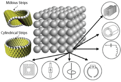
Figure 1 Möbius strips formed by graphene nanoribbons exhibit negative index properties suitable for high Q-factor microwave components.
Metamaterial Möbius strips (MMS) have captured the interest of research scientists because of their distinctive properties, such as topological symmetry, which is conserved when the system undergoes an alteration such as deformation, twisting and stretching; and a negative index of refraction (i.e., 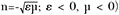 . Figure 1 shows typical negative index (ε < 0, µ < 0) Möbius strips formed by graphene nano-ribbons that are used to create topologically-induced high Q-factor components with desirable electromagnetic properties. Unlike conventional materials, which interact with electromagnetic waves based on their chemical compositions, the properties of negative index materials (NIM), otherwise known as metamaterials, come from their geometric topological structures.
NIMs, as shown in Figure 1, are artificial engineered topological structures intended to modify the bulk permeability and permittivity of the medium. This is realized by constraining the size of periodically unit cell NIMs structures size to typically less than the wavelength of incident EM waves. It is interesting to note that by changing the position, orientation and excitation of the NIMs structures, important parameters such as permittivity, permeability, refractive index, transmission, reflection, impedance and coupling can be tuned and optimized for desired applications. There are many ways to vary the properties of NIMs, such as using ferrites, liquid crystals, frequency-selective surfaces and hybrid-NIMs, or by manipulating their lattice structures.
Figure 2 shows the typical characteristics of a medium that explains the properties of natural and artificially engineered composite material.1 The third quadrant describes the properties of a left-handed medium that posses NIM characteristics. The evanescent-mode energy storage and resonance characteristics of the third-quadrant material enables potential applications in electronics, medical, space and optics. Hence, it is important to understand its fundamental EM dynamics for the design of NIMS resonator based electronic signal sources. It is important to note that exact characterization of εand µ of a NIM structure is a challenging task for wideband frequency operation.
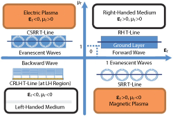
Figure 2 Typical representation of a medium; the third quadrant explains NIM properties.
In addition to this, the justification for using effective constitutive parameters (ε < 0, µ < 0) provides a convenient means to understand the behavior of the artificially engineered NIM structures without considering, in detail, the local EM-field distribution. To establish faithful values for these parameters, numerous methods have been reported, but none of them provide exact solutions because of hypotheses concerning the NIM’s tiny size, and they neglect coupling. The general isotropic medium model assumes that the induced electric and magnetic dipoles are mutually independent, but in reality this is not always the case. NIMs are intrinsically anisotropic and sometimes bi-anisotropic because of the geometry and orientations of their structures.
For example, split rings (SR) as shown in Figure 3, typically used in NIMs, exhibit simultaneous electric and magnetic responses; i.e., their corresponding dipoles are coupled.5 This leads to cross coupling between the electric and magnetic field in SR inspired NIM structures. Therefore, it is not recommended to discount the magneto-electric coupling that depends on the shape of inclusions, wave polarizations, excitation and orientation of NIM structures. To account for both asymmetric reflection and magneto-electrical coupling, the bi-anisotropic medium model can be used.
Figure 3 shows typical NIM circular and square split ring structures. Their sizes and the distances between them are kept smaller than a wavelength (λ). Under these conditions, an SR-NIM structure may present bulk properties that can be characterized by a macroscopic model, with parameters ε and µ. The expression n is given by
Figure 3 Typical SRRs and NIM construction with closed SRR wire structure: circular split ring (a) and rectangular split ring (b).

From (1), a positive sign is used for n when ε, µ > 0, whereas a negative sign is used when ε, µ < 0. The assumption of positive index (n > 0) implies that the index n is a scalar, and does not depend on frequency. But in reality, this is not always true. The energy of the field (W), where W =εE2+µH2, would be a negative value when ε and µ are negative, and this is not possible; hence εand µ are bound to depend on frequency and fall into complex domain.2 The unified expression of energy W can be described by
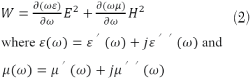
From (2), the electrodynamics of negative index materials (n < 0; ε< 0 and µ < 0) provide a positive W value for a very broad class of dispersive materials characterized by ε(ω) and µ(ω), exhibit dependency on frequency.
Any material supporting a single propagating mode at a known frequency usually exhibits well-defined n, whether the material is homogeneous/continuous or not. But it is not easy to assign z to a non-homogeneous material, because z strongly depends on the surface termination and overall size of the material.1 The classical homogenization theories are typically valid when the unit-cell size is insignificant with respect to wavelength (the zero frequency limits) and thus might be expected to result in a poor description of negative index materials. The key supposition is, if the wavelength of the incident wave is much larger than the size and spacing between the NIM’s unit cell elements then it is possible to perform homogenization, and to obtain a value of z within an acceptable range of error.2,3
Assuming the size of a NIM structure is much smaller than λ/10, the homogenization theory can be applied to topology inspired Möbius strips. The averaging of Maxwell’s equations over small volumes (with respect to a wavelength) can be performed to obtain an analogous uniform continuous harmonized medium described by effective constitutive parameters (ε and µ). It is possible to retrieve values for the complex n and z of inhomogeneous periodic negative index Möbius strips (NIMS) structures with prior information about the termination of the NIM unit cell, and the phases and amplitudes of the waves transmitted/reflected from the NIMS sample. The challenge is that if the NIMS structures are not symmetric along the wave propagation direction, two different values of z are retrieved corresponding to two incident directions of propagation. This ambiguity in the computation of z leads to a fundamental ambiguity in the definitions of ε and µ, which increases as the ratio of unit cell dimension to wavelength increases.
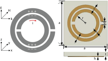
Figure 4 Typical SRR unit cell showing the inner and outer asymmetric rings.
The simplest theoretical formulation of a SR inspired NIM can be deduced from an equivalent circuit model that gives insight into the relationship between the physical properties and geometric parameters of SRRs as shown in Figures 3 and 4. Analytical values of the constitutive parameters (εzz, µyy, ξ0) are given by 5, 13, 17
where 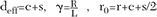 and rext=r+2c+s; L and Cpull are the total inductance of the SRR and the capacitance between the rings respectively.
From the equivalent circuit model, RR behaves as a resonant LC circuit, and that the frequency of the resonance is given by
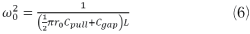
L and Cpull can be calculated from the analytical equations reported by Marques et al.17 Cgap is the capacitance of the gap, if the gap is narrow, its capacitance can be analytically written as18
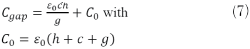
From Marques et al.,17 L = 3.9287 × 10⁻⁹ H, Cpul = 1.6806 × 10⁻¹¹ F, Cgap = 4.1557 × 10⁻¹⁵ F and R = 0.4901 Ω at the frequency of resonance. The poor accuracy of the analytical method for constitutive parameter calculation given in (3) through (7) and the deficiency in complex modeling of thicker structures limits its validation. The alternative approach is a retrieval technique based on the extraction of S-parameters. The advantage of the retrieval method is that it can be used for simulated and measured S-parameter data; thin samples (in the propagation direction) are preferred to minimize the errors.
In general there are three methods used for the determination of effective constitutive parameters based on applications and acceptable errors.3 The first method is to numerically calculate the ratios of the EM field inside NIM structure. This approach is good for numerical simulations, but not appropriate for experimental measurement.4 The second method calculates the effective constitutive parameters by using analytical models of NIM structures including the numerical averaging of fields; but, this technique is not suitable for complex NIM structures.5 The third method is a retrieval technique based on the inversion of scattering data (S-parameters) of a finite slab, called the Nicolson–Ross–Weir (NRW) procedure.6,7
The NRW method was developed for the measurement of complex permittivity and permeability of natural materials and recently applied to NIMs.1-20 The problem with NRW method arises in cases where topology-driven NIM structures undergo asymmetric reflections. Smith et al.,2 reported a modified approach to resolve this issue of asymmetric reflections by using averaged values of reflection coefficients. The isotropic medium model cannot duplicate this property, as it is intrinsically symmetric, hence it is important to understand the EM dynamics of SR inspired NIM media that inherently possess reflection asymmetric structures (S11 ≠ S22).21
EM Dynamics of Media
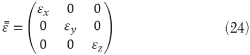
The fundamental equations describing EM waves in a biaxial anisotropic medium (or simply called biaxial) are more complex than the isotropic equations. Isotropic materials have a single permittivity ε. In an isotropic media, the constitutive relations that relate the electric flux density  to the electric field intensity
  and the magnetic flux density
  to the magnetic field intensity
  are given by

From (8), ε describes the medium’s electrical properties and µ describes its magnetic properties. The time-harmonic forms of Maxwell’s equations for isotropic media are given by
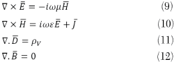
A medium is called electrically anisotropic if =  · , where is the permittivity tensor. A medium is magnetically anisotropic if =
  ·, where is the permeability tensor, note that and are no longer parallel. A medium can be both electrically and magnetically anisotropic. In the electrically anisotropic case, and are no longer parallel, and is given by
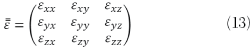
For example, crystals, in general, are described by a symmetric permittivity tensor; there always exists a coordinate transformation that transforms the symmetric matrix to a diagonal matrix as given by
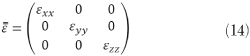
From (14), the new coordinate system is called the principal system, and the three coordinate axes are called the principal axes. For a cubic crystal where εxx=εyy=εzz=ε, the crystal is isotropic.
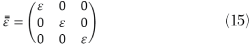
For tetragonal, hexagonal and rhombohedra crystals two of the three εare equal; such a crystal is called uniaxial. Uniaxial anisotropic materials have two different permittivity values. They have the same permittivity along two dimensions and a different permittivity along the third dimension. An unrotated uniaxial permittivity tensor can be written as
From (16), the principal axis that is different (exhibits anisotropy) is called the optical axis (z-axis is the optical axis), and there exists a two dimensional degeneracy. If εzz>ε, the medium exhibits positive uniaxial behavior, and if εzz<ε, the medium shows negative uniaxial characteristics.
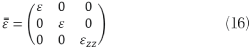
If εxx≠εyy≠εzz, the crystal is biaxial. Examples of biaxial crystals are orthorhombic, monoclinic, and triclinic. The defining property of electrically biaxial media is the permittivity tensor .
If the medium is biaxial anisotropic, the permittivity and permeability of medium take on a tensor form. From (8), the set of matrix equations can be described by
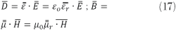
where r and r are relative permittivity and permeability tensors, respectively. From (17), the change in constitutive relations also affect Maxwell’s equations (9)-(12) in the medium,
The NIM exhibits properties of a bi-anisotropic medium, provide coupling between electric and magnetic fields. The constitutive relations for a bi-anisotropic medium are given by
Figure 5 Wave vector surface: unrotated biaxial medium (εx, εy, εz) = (2, 8, 4), plotted over 0 ≤ θ ≤ π and 0 ≤ φ ≤ π.
A bi-anisotropic medium placed in an electric or magnetic field becomes both polarized and magnetized. Almost any medium in motion becomes bi-anisotropic. The first cases of bi-anisotropic materials were indeed moving dielectrics and magnetic materials in the presence of electric or magnetic fields. The topics of moving NIMs and their constitutive relations are the subject of relativistic electromagnetic theory, and can lead to Casimir effect (anti-gravity).15 The permittivity described in (16), represents an unrotated uniaxial medium with its optic axis along the z-direction.
Biaxially anisotropic materials have three unique values in the permittivity tensor and they have two optic axes. An unrotated biaxial permittivity tensor is given by
where εx≠εy≠εz. From (8), principal axes of a biaxial medium are aligned with the Cartesian coordinate system.
For a better understanding, Figure 5 shows the plots of the unrotated biaxial medium; the inner surface is called the “a-wave vector surface” and the outer surface is the “b-wave vector surface”. The intersecting line is one of the optic axes, it can be seen from Figure 5 that the optic axis intersects the wave vector surfaces at some point and the “b-wave wave vector surface” is at a local minimum at the point of intersection.10 If the biaxial medium is arbitrarily oriented with respect to the coordinate system, the permittivity tensor representation would be complex and not as simple described in (8).
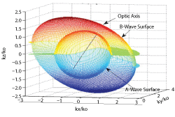
Figure 6 Wave vector surface: rotated biaxial medium (εx, εy, εz) = (2, 8, 4), rotated by (ψ1 ψ2) = (30˚, 75˚).
The evaluation of the tensor for an arbitrarily oriented biaxial medium is given by applying rotations to the tensor in (8); the wave vector surfaces are shown in Figure 6. Studying the wave vector surfaces of the unbounded region shown in Figures 5 and 6 give insight into how the wave influences the important parameters (ε, µ, n, z ) in the composite NIM structures, which are intrinsically anisotropic and sometimes bi-anisotropic due to geometry and structural orientations.
Constitutive Effective Parameters
Most of the NIMs presented over the past several years are artificially engineered SR-inspired periodic structures.1-27 It is convenient to extract the parameters from a unit cell of periodic structures through numerical approaches. It has been demonstrated that under the condition of long wavelength, a material with a periodic structure can be viewed as a homogeneous medium and its properties can be described by the effective medium parameters. The properties of a periodic structure can be determined from the transfer-matrix (T) associated with the fields of a unit cell.
NIM structures fall into the category of anisotropic and bi-anisotropic (cross-coupling exists between electric and magnetic fields in bi-anisotropic) due to their orientation and special geometric structures. When computing the effective parameters of NIM structures, magneto-electric coupling is a critical parameter. The simplified approach to retrieve the coupling parameter of a bi-anisotropic material from S-parameters is based on transfer-matrix method. The transfer-matrix method has been used to retrieve the effective EM parameters of homogeneous and non-homogeneous materials.1,2
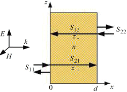
Figure 7 Plane wave incident in the x direction into a bi-anisotropic slab.13
Figure 7 shows a typical of bi-anisotropic slab of thickness d placed in air, illustrating the direction of S-parameters. For a material consisting of periodic structures, there is a phase advance per unit cell, which can be defined by the periodicity.13
Chen et al.,16 extracted effective constitutive parameters of bi-anisotropic negative index material from S-parameters for various wave polarizations using a numerical approach for a plane wave polarized in the z direction and incident in the x direction. Figure 8 shows the triplet  based on a right-handed coordinate system, containing an electric and magnetic field.
As shown in Figure 8, the plane wave polarized in z- axis propagates along the x- direction, the electric fields in the z-direction will induce magnetic dipoles and the magnetic fields in the y- direction will induce electric dipoles due to the asymmetry of the inner and outer rings. It means that electric dipoles cannot only be excited by the E-fields but also by the H-fields. Similarly, magnetic dipoles cannot only be excited by the H-fields but also by the E-fields.
Assuming that medium is reciprocal and that the harmonic time dependence is e-iωt, the constitutive relationships are given by19
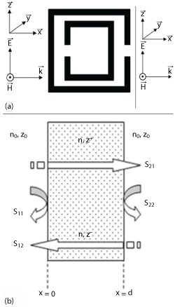
Figure 8 Planar SRR structure (a) and homogeneous bi-anisotropic material slab suspended in air, with S-parameters used to determine forward and backward wave impedances (b).3
where , , and , are electric field, magnetic field intensity, and flux density; ε0 and µ0 are the permittivity and permeability in a vacuum; c is the speed of light in vacuum; and the other four quantities are dimensionless and are unknowns. When a plane wave polarized in the z-direction is incident in the x-direction, only two components of EM-fields (Ez and Hy) and three EM parameters (εzz, µyy, ξ0) are included.
The numerical formulation is done for the determination of the forward and backward wave impedances entailed by parameters εzz, µyy and ξ0, since the unknown four quantities εxx , εyy , µxx , and µzz are not related to the bi-anisotropic structure in Figure 8b. From (18)-(19):
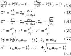
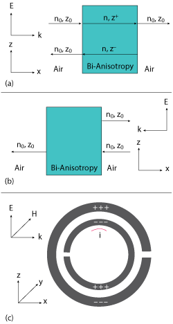
Figure 9 Signal flow of a homogeneous bi-anisotropic slab placed in open space, for the calculation of S-parameters for plane waves incident in the +x (a) and –x (b) directions; NIM unit cell (c).
where Ez and Hy are the z and y components of  and
and  ; kx and k0 are the wave number of the wave propagating in the x direction and in free-space, Z+ and Z- are wave impedances inside the medium for forward
 ![]() and backward
and backward  propagations; z+ and z- are normalized (or non-dimensionalized) wave impedances in respective directions; Z0 is the wave impedance (or intrinsic impedance) in air; and n is the refractive index of the negative index structure.
From (30),(31), bi-anisotropic NIM structure samples exhibit different values of wave impedances for forward and backward wave propagation.2,20 The non-homogeneous periodic NIM structure does not exhibit distinct impedance values because the ratio of  varies periodically throughout the structure. This variation is negligible if the NIM structure unit cell sizes are small relative to a wavelength. It is important to note that the lack of a unique definition for z± indicates that the values of εand µ retrieved are not assignable but can be applied if the NIM formed by the periodic structure is always terminated in the same location of the unit cell. The surface termination has an increasing influence on the scattering properties of the structure as the scale of inhomogeneity increases relative to a wavelength.
It has been demonstrated that under the long wavelength condition, materials with periodic structures can be viewed as homogeneous and their properties can be described by the effective medium parameters. The properties of a periodic structure can be determined from the transfer-matrix (T) that is associated with the fields of a unit cell. We express the fields in the form of a vector  , where and are the complex amplitudes of the electric and magnetic fields located on the left-hand and right-hand faces of a slab. The magnetic field is a reduced field with the normalized form ' = iωµ. The relations of fields on two sides of a slab can be expressed as

where α is the phase advance per unit cell which relates the fields on its two sides. T is the one dimensional transfer matrix of a NIM slab
with k0 being the wave number of light in free space, z being the wave impedance of a slab and n being the refractive index. From (35) and (36), the dispersion relation is given by solving
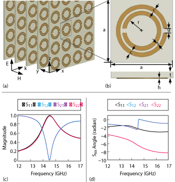
Figure 10 A typical bi-anisotropic structure: array of SRRs printed on substrate with metallization (a) SRR unit cell (b) magnitude (c) and phase (d) of S-parameters.13
The elements of the transfer matrix can be expressed in terms of S-parameters.
Figure 9 shows the schematics of a homogeneous bi-anisotropic material slab that is placed in an open space. There are two different situations to be considered, i.e., wave incidence in the +x and −x directions. After applying the boundary continuous conditions, it is easy to obtain the expressions for the S-parameters by using the transfer matrix method.20 When the incidence is in the +x direction as shown in Figures 7 and 9a, the corresponding reflection (S11) and transmission (S21) coefficients are
where l is the thickness of the homogeneous bi-anisotropic material slab and k0 is the wave number of light in free space. For the case when the incidence is in the −x direction, as shown in Figure 9b, we obtain the corresponding reflection (S22) and transmission (S12) coefficients as
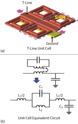
Figure 11 SRR loaded T-line unit cell (a) and equivalent lumped LC model (b)
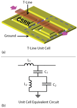
Figure 12 CSRR loaded T-line unit cell (a) and equivalent lumped LC model (b).
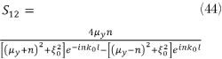
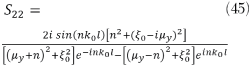
Figure 13 Typical broadside-coupled split ring resonator (a) and equivalent lumped circuit representation (b).22
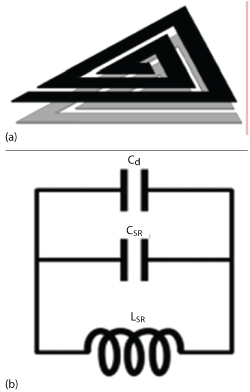
Figure 14 Layout of the BCTSR (a) and equivalent lumped circuit (b).
From (43)-(45), S21 is equal to S12, but S11 is not equal to S22. There are three independent equations for the three unknowns (n, µyy and ξ0). By solving analytically (43)-(45), the expression for refractive index n is given by
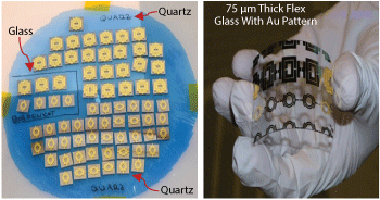
Figure 15 Metamaterial resonators fabricated on glass and quartz.
From (36), using the condition of determinant (T)=1, and substituting (38)-(41):
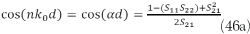
It is understood that when S11 is equal to S22, (46) will degenerate into a standard retrieval form.2 The refractive index n can be obtained from the implicit expression (46), which has many solutions for n to the different branches of the inverse cosine. When solving for n from (46), one must determine one branch from many branches of solutions. For a passive medium, the n must obey the condition n″=Im(n)≥0. After computing n, the other constitutive parameters are
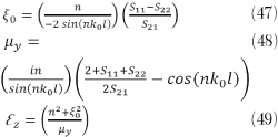
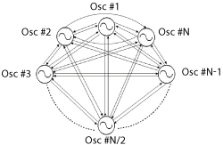
Figure 16 A typical N-coupled N-push oscillator topology.29
Consequently, impedances z+ and z− can be obtained from (29)-(30). For a passive medium, the following conditions should be satisfied: z+'=Re(z+)≥0, z-'=Re(z-)≥0.
From (47)-(49), retrieved effective constitutive parameters can be assigned to the NIM structure; however, a variety of artifacts exists in the retrieved material parameters that are related to the NIM structure’s inherent inhomogeneity. The artifacts in the retrieved material parameters are particularly severe for NIM structures that make use of resonant elements, as large fluctuations in the index and impedance can occur, such that the wavelength within the material can be on the order of or smaller than the unit cell dimension. The retrieval technique based on analyzing the S-parameter of a finite slab can suffer from unphysical anti-resonances with negative imaginary parts for some of the parameters. These anomalies could be due to periodicity of the structure and spatial dispersion.11,12
An example of this behavior can be seen in the retrieved imaginary parts of εand µ, which typically differ in sign for a unit cell that has a magnetic or an electric resonance. In homogeneous passive media, the imaginary components of the material parameters are restricted to positive values. This anomalous behavior vanishes as the unit cell size approaches zero.2 For a homogeneous or symmetric material, the value of z will be unique, while it will result in two different values for an inhomogeneous or asymmetric material. The impedance  is an intrinsic parameter which relates the electric field to the magnetic field.
Figure 17 Bimodal distribution consisting of the sum of two Lorentzians.17
From (35), two equivalent expressions for the impedance of a slab can be obtained by
from (37) and (50)
The two roots of (51) correspond to the two propagation directions of a plane wave. Substitution of (38)-(41) into (50) leads to
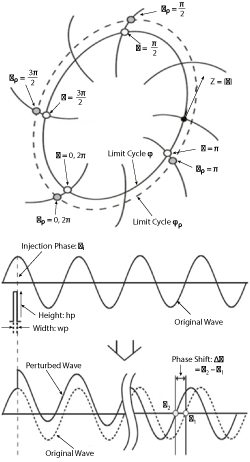
Figure 18 Typical phase injection mechanism in a Möbius strip resonator due to perturbation at the ith node.
From (51) and (52), the characteristic impedance in terms of S-parameters associated with a metamaterial having bi-anisotropic structures is obtained. For a passive medium the impedance needs to satisfy the conditions (z+)'≥0 and (–z-)'≥0 , where ( )'denotes the real part operator.
For an example, a typical array of SRRs printed on substrate and unit cell is shown in Figure 10. As illustrated in Figure 10a, a plane wave is incident in the x direction and polarized in the z direction. The dimensions are α= 3 mm, r = 0.74 mm, c =0.2 mm, s = 0.1 mm, g = 0.2 mm, t =0.3 mm, h = 35 mm; and the substrate permittivity is ε0, for simplification.13
It can be seen from Figures 10b and10c that S12 is equal to S21 and the magnitudes of S11 and S22 are almost the same, while the phase of S11 is different with that of S22. In this case, the application of the standard retrieval method1 will lead to an inaccurate result. The discrepancy in phase of S-parameter measurements is because of the fact that the NIM’s cells are not infinitely small compared to the incoming wavelength, causing spacial dispersion.
Assuming that there is a plane wave propagating in the direction of +x, polarized in the +z direction. The constitutive relationship between electric field and magnetic field can be described as
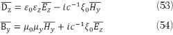
With the substitution of (53)-(54) into Maxwell’s equations (18)-(19):

From (13), the index (n) can be given by

For a passive material, the roots have to be chosen properly to guarantee the condition Im(n)≥0 Otherwise, the exponentially growing solutions will occur, which violates energy conservation. The impedances of a bi-anisotropic material for wave propagation in the right-hand or left-hand directions are Z±, the values of which are given by the equations
. 
From Maxwell’s equations (18)-(21), the formulas of the impedance and effective parameters can be obtained,
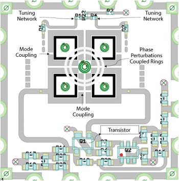
Figure 19 Typical layout of 25 GHz oscillator using Möbius coupled resonator.
The refractive index and impedances for a bi-anisotropic medium can be obtained from (46) and (52). The expressions for the effective electromagnetic parameters (εz, µy and ξ0) and impedance associated with the bi-anisotropic structure are obtained from (58)-(60), and can be used for designing NIMS resonators for next generation energy efficient signal sources.
NIMs Inspired Resonator For Oscillators
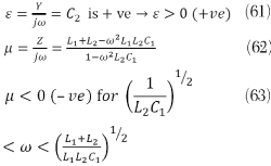
A NIMs resonator can be classified into two types: resonant type and non-resonant type: examples are the split ring resonator (SRR), and left handed (LH) transmission line (T-line). Resonant type metamaterial exhibits larger dynamic range for material parameters (εr < 0, µr < 0), while non-resonant type metamaterial offers wide bandwidth and lower loss. Traditional metamaterial T-lines can be categorized into resonant type and non-resonant type, represented by the SRR/(complementary SRR) CSRR loaded T-line, and composite right/left handed (CRLH) T-line, with corresponding layouts shown in Figures 11 and 12, where C and L are per-unit length capacitance and inductance that determine the T-line metamaterial properties. For a T-line loaded with an SRR (see Figure 1), L1 and C2 are linked with T-line, whereas C1 and L2 are linked to magnetic coupling. Figure 11 shows the typical split ring resonator and NIM construction.
The physical properties in Figure 11 are given by:
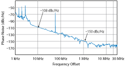
Figure 20 Measured phase noise of the 25 GHz oscillator shown in Fig. 19.
From (61) and (63), Re (µ) is negative and Re (ε) is positive. For (ε>0, µ<0), propagating waves become evanescent waves, therefore energy cannot propagate through the resonator and is reflected back to establish a standing-wave.
Figure 21 Ring resonator (a) Möbius strip (b) and equivalent LC representation consisting of L and C along the transmission line (c).
As a result, the SRR loaded T-line structure stores the energy and forms a high-Q resonator tank circuit for a low phase noise oscillator application. Similarly, for a T-line loaded with a CSRR (see Figure 12), L1 is associated with the T-line, while C1, C2, and L2 account from electric coupling of the CSRR to ground.
The physical properties in Figure 12 are given by
From (64) and (66), Re (µ) is positive and Re (ε) is negative. In this case (ε< 0, µ > 0), and electric plasma is formed, where propagating waves become evanescent waves, hence, energy cannot propagate through the resonator either and is reflected back to establish a standing-wave. As a result, the CSRR loaded T-line can also be used to form a high-Q resonator.
Figure 13a shows the structure of the broadside-coupled split ring resonator, there are two relative slips Sx and Sy between the two broadside coupled rings. Figure 13b shows the corresponding equivalent circuit, where L and R are the equivalent inductance and resistance, respectively, C0 is mutual capacitance between the two rings and Cs is the capacitance of the split. As shown in Figure 13a, the tuning can be realized with minor slips along and perpendicular to the gap direction of two broadsides coupled rings.22 Figure 14a shows the layout of the broad coupled split ring (dark region denotes etching on the signal plane, and light region denotes broadside coupled triangular SR etched on ground plane), and Figure 14b shows the equivalent lumped circuit.
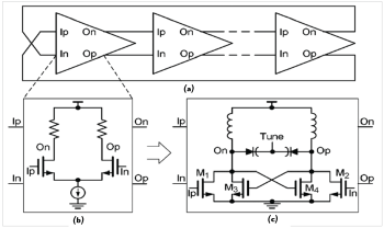
Figure 22 Ring oscillator structure (a) active gain stage (b) and LC-boosted gain stages (c).32
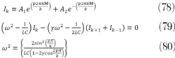
For the validation of reported research work, resonators are fabricated on low loss quartz and borosilicate material. As shown in Figure 15, the metal structures are processed on top of quartz wafers (diameter D = 150 mm). The fabrication process uses a double-side coating of the substrates with a sputtered metal gold (Au) metallization. Unlike the SRR/CSRR depicted in Figure 15, the geometry of negative index Möbius strips (NIMS) is conformal, continuous, and maps one-to-one onto itself. These unique properties of NIMS permit EM coupling in such a way that a signal coupled to the loop does not encounter any obstructions when travelling around it, emulating an infinite transmission line; hence providing a large group delay and high Q-factor. In this paper, the oscillator circuit uses a negative index (εr <0, µr <0) NIMO (Negative Index Möbius Oscillator) circuit for low cost high performance solution.
Examples
Signal Source
Möbius metamaterial inspired (MMI) structures are artificially constructed media on a size scale smaller than a wavelength of the external stimuli. They can exhibit a strong localization and enhancement of fields, which may provide novel tools to significantly enhance the sensitivity and resolution of sensors, and open new degrees of freedom in sensing design.1-10 A detailed discussion about MMI structure characteristics is given in part 1 (MWJ May 2016 Issue), this issue (part 2) presents mainly their applications in high frequency signal sources and sensors, as well as the challenges and prospects.28
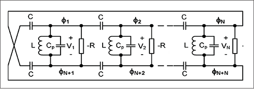
Figure 23 Typical negative index Möbius connected LC-ring oscillator.33
From part 1 (MWJ May 2016 Issue, Equations 2 to 6, Ref 28), the Möbius transformation can be used for reducing the complexity of a system of N-coupled oscillators.28 Figure 16 shows the typical N-coupled N-push oscillator topology for the purpose of analysis.29
Globally, coupled oscillators have been used to model many diverse systems in physics, biology, chemistry, engineering, and space science. The system of coupled oscillators exhibits complex behavior because each individual unit influences the characteristics of other units. The phase dynamics of the N-coupled oscillator shown in Figure 16 is described by29
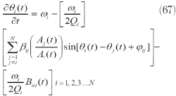
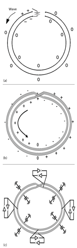
Figure 24 Oscillation based on the Möbius effect: open loop differential ring (a) Möbius connected differential ring (b) and practical tunable Möbius connected differential oscillator circuit (c).37
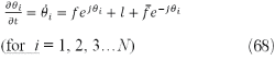
where Ai(t), θi(t),ωi, and Qi are the amplitude, phase, free-running frequency, and Q factor of the ith oscillator, Bni corresponds to the phase fluctuations; and βij and φij are the coupling parameters between ith and jth oscillators.
From (67),
where f is any smooth complex-valued 2π-periodic function of the phases θ1,… θN and over bar  is the complex conjugate.
The coupled-oscillator system shown in Figure 16 tends to collective synchronization and lock to a common frequency, despite the difference in oscillator natural frequencies. However, an accurate solution of (67) and (68) becomes difficult due to the nonlinearity and large number of variables associated with coupled-oscillator systems.
An alternative means to solve this is by reducing the complex dynamics to phase models assuming the couplings among oscillators are sufficiently weak such that when they are uncoupled, their phases advance at constant ‘velocities’ (natural frequency). The functions f and l given in (68) may depend on time and on any auxiliary state variables in the system, assuming such system is sinusoidally coupled because the dependence on i occurs solely through the first harmonics ejθi and e-jθi ).30 This particular class of dynamical systems (68) can be reducible by a Möbius transformation in the form.31

for I = 1, 2, 3…N, where Mt is a one-parameter family of Möbius transformation and ϕj is a constant (time-independent) angle. The time-t flow map is an orientation-preserving homeomorphism that exhibits a Möbius map.
From (67) and (68), the distribution of natural frequencies for N→∞ s given by the sum of two Lorentzian distributions l (ω) [31]:
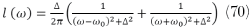
where ∆ is the width parameter (half-width at half-maximum) of each Lorentzian and ±ω0 are their center frequencies, as depicted in Figure 17.
From (70), the challenges are the minimization of frequency detuning (proportional to the separation between the two center frequencies) and AM-PM conversion noise. For low noise oscillator applications, resonator Q-factor is important parameter. Resonator networks formed with Möbius strips are conformal, continuous, and map one-to-one onto itself; therefore, signals coupled to strips do not encounter any obstructions while travelling around them in such a way that a loop made of strips acts like an infinite transmission line. This arrangement enables a large group delay and improved Q-factor, which is promising for filter and oscillator applications. Möbius strips can have more than 1-twist (Figure 13, MWJ May 2016 Issue part 1, Ref 28). The 3-twisted Möbius strip has a trefoil knot as the boundary curve and so on. It is interesting to analyze the geometric phase of multi-knot non-orientable (Möbius) surfaces and their connection with nonlinear dynamical systems. This may provide a diagnostic analysis in abnormal neural oscillations and synchrony in schizophrenia.
Figure 18 illustrates a typical phase-injection mechanism using phase-perturbation at the ith node on a Möbius strips resonator based frequency generating electronic circuit. The Q-factor (QL) of the resonator is29
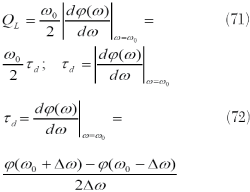
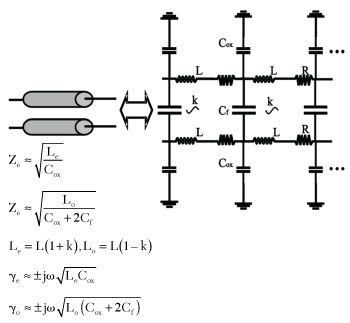
Figure 25 Lumped representation of coupled stripline model (Ze, Zo are even and odd mode impedances; γe, γo are even and odd mode propagation constants; Le, Lo are even and odd mode lengths).36
where φ(ω) is the phase of the resonator impedance and τd is the group delay. The effective inductance of the Möbius strips varies with the current/voltage passing through them, building the evanescent field for a higher quality factor:
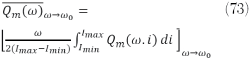
where Imin and Imax are the minimum and maximum currents, and Qm(ω,i) is the instantaneous quality factor at frequency ω and current i flowing through the Möbius strips resonator.
From Figure 18, the locking condition is given by
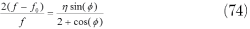
From (74), the locking range is restricted by the phase shift30
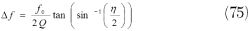
where f0, Q, and η are the resonant frequency, quality factor of the LC tank, and the injection ratio (iinj/IDC) respectively.
Using Equations (71)-(75), a 25 GHz multi-knots Möbius-strips resonator based oscillator is designed and validated. Figure 19 shows the circuit layout of tunable oscillator using multi-knots Möbius-strips resonators that support multi-injection nodes, thereby minimize detuning and provide a mechanism to suppress noise. The influence of phase-injection (perturbations) at different nodal points on the Möbius strips resonator are discussed for improving the tuning-range and phase noise performance of frequency generating circuits. The PCB is fabricated on an 8-mil thick Rogers substrate with a dielectric constant of 2.2.
As shown in Figure 19, the Möbius strips resonator increases evanescent mode field energy conservation due to the invariance of solutions for strips under a 2π rotation with a definite handedness. The resonator coupling coefficient βj depends upon the geometry of the perturbation:
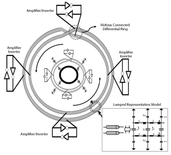
Figure 26 Möbius connected rotary wave oscillator, with distributed coupled lines represented as the continuous limit of the multi-section lumped LC circuit.
where Ea and Ha are the electric and magnetic field produced by the Möbius strip, and Eb and Hb are the corresponding fields due to perturbation of nearby adjacent resonators. The subscripts ‘e’ and ‘m’ denote electrical and magnetic coupling.
The oscillator circuit works with a DC bias of 5 Volts and 68 mA. Measured output power is typically -6 dBm. Figure 20 shows measured phase noise of -109 dBc/Hz at 10 kHz offset with an output power of 6.73 dBm and 500 kHz tuning. The major drawback of this topology is limited tuning and mode-jumping.
For practical applications, output power, frequency stability, and tuning range need to be improved. These problems can be partially or fully fixed by understanding the phasor relationship between ring and Möbius strip resonator. Figure 21 shows the typical representation of ring and Möbius strips resonators, and the equivalent LC representation consisting of inductors and capacitors along the transmission line. By virtue of the Möbius transformation, strips exhibit large group-delays, well suited for microwave resonator applications.
The electric currents on the ring resonator in Figure 21c can be formulated by a periodic boundary condition of the form described by

where Ik represents the electric current around the nth closed loop on the periodic ladder structure of k-elements. The boundary condition of the general form shown in (77) governs that Ik is a conserved quantity that gives invariance to solutions under a 2π rotation with a definite handedness. The non-dissipative wave equation of the LC network for the kth element is
Figure 27 Layout of a 12 to 18 GHz oscillator using an evanescent mode metamaterial Möbius strip resonator network realized using 8 mil RT/Duroid 5880 with εr = 2.2. The oscillator measures 0.75" × 0.75".
where p is an integer specifying the normal mode and γis the mutual coupling coefficient (mutual inductance ‘M’=2γL). From (77)-(80), for even value of k, there are k-1 eigenvalues, including (k-2)/2 degenerate doublets and one singlet.
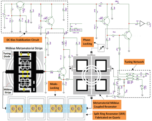
Figure 28 28.5 GHz NIMO oscillator.
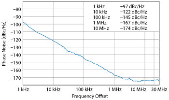
Figure 29 Measured phase noise of the 28.5 GHz NIMO oscillator shown in Fig. 28.
A typical ring resonator, whose eigenfunctions satisfy (17), defines a distinct inner and outer surface of the ring, shown in Figure 21a. Figure 21c shows a topological transformation resulting in a Möbius strip resonator, whose current dynamics formulated by applying twisted boundary condition as

From (81), a simple topological transformation on the resonator ring (see Figure 21b) results in a sign reversal of current (Ij) upon a 2π rotation of the solutions, and a 4π rotation is now required for invariance of the eigenfunctions. Note that the eigenfunctions satisfying the condition for twisted boundary are of the same form as (77) provided that the mode indices are given half-integral values (p = 1/2, 3/2, 5/2,…(k-1)/2) relative to a ring consisting of identical components. The dispersion relation for the Möbius ring is the same as (80), however, the wave-vectors are shifted by

From (80)-(81), the two distinct topologies shown in Figures 21a and 21b can be considered a complementary pair related by a single transformation. The eigenfunctions of the Möbius resonator form an orthogonal basis set, presenting an interesting possibility for the design of metamaterials for multi-phase oscillator circuits. The inherent multi-phase, multi-mode nature of the Möbius strip provides additional degrees of freedom relative to traditional designs for generating multi-phase and quadrature oscillators. These are essential modules of many electronic systems, such as image rejection demodulators in wireless transceivers, half-rate clock-data-recovery (CDR) circuitry in high-speed optical receivers, phased-arrays, direct-conversion transmitters, and fractional-N frequency synthesizers.
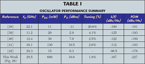
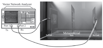
Figure 30 Typical measurement setup for wireless power transfer efficiency.53
Figures 22a and 22b show a typical ring oscillator. It exhibits multi-phase but it suffers from high phase noise.31 The LC-boosted ring oscillator shown in Figures 22a and 22c minimizes the noise but is still inferior to a single-stage LC oscillator, largely due to the tradeoff between phase noise and phase error. Strong coupling between the gain stages (implying large-coupling MOSFETs) can minimize the phase errors; however, large coupling MOSFETs increase noise and power consumption.31 In all multiphase LC oscillator configurations, MOSFETs play a dual role; they compensate LC tank energy loss and they couple LC tanks together to maintain a desired phase relation.32 The second role, however, deteriorates phase noise, especially 1/f (flicker) noise up-conversion.33
These problems can be partially, or fully, overcome by replacing the MOSFETs with metamaterial Möbius connected high order LC ring resonators in a distributed topology, as shown in Figure 23. The resonant frequency of metamaterial (-ve index) LC-ring resonators increases with the number of stages N as compared to right-handed (+ve index) LC-ring resonators. Therefore, the metamaterial LC-ring resonator is well suited for high frequency generation. The MOSFETs act as negative resistance generating devices, needed only for compensating the losses of the LC-ring resonators, implying that current from the MOSFETs is always injected into the resonator in phase with the voltage and does not resonate with LC resonator components. For an N-stage distributed LC-ring oscillator, the phase noise scales as 1/N, while the power consumption increases linearly with N. This allows synthesizing multi-phases, while maintaining the identical figure of merit (FoM) as a 1-stage LC oscillator.34
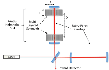
Figure 31 Typical experimental setup for measuring gravitational waves.54
The main challenges of these topologies are mode selection and maintaining desired phase relationships. In addition, the number of noise sources increases linearly with N; the total phase noise should be proportional to 1/N, but this no longer holds under large signal drive level conditions. The alternative approach is a wave-based Möbius oscillator. The energy recycling nature of Möbius strips allows very high frequency oscillation with minimal power consumption for a given class of frequency generating circuits.
Figures 24a and 24b show the differential open ring and closed cross-connected ring, respectively. When the voltage source connected in Figure 24a is replaced by a cross-connection of the inner and outer conductors, it leads to a signal inversion. If there were no losses, a wave could travel on this differential ring indefinitely, providing a full clock cycle for every other rotation of ring through the Möbius effect.35 In real applications, however, multiple anti-parallel inverter pairs are added to the line shown in Figure 24c to overcome losses and provide rotation lock in the Möbius connected differential ring.
Figure 25 shows the lumped equivalent of coupled stripline used for the Möbius ring described in Figure 24.36 As shown in Figure 25, coupled lines support even and odd mode propagation. The even mode (fast wave mode) is when the two lines are excited with the same signal; as a result, the coupling capacitance Cf between the two lines has no effect on the propagation constant γ. The odd mode (slow wave mode), is obtained as the line pair is excited differentially, so the coupling capacitance between the two lines has a doubling effect on the propagation constant of this mode. For the resonator application, slow wave propagation is of interest and care must be taken to suppress even mode propagation.
Figure 26 shows the method for achieving stable oscillation. Inverters across the lines provide gain and theoretically force the line to operate differentially; varactor diodes and the center ring provide even mode cancellation.35-37
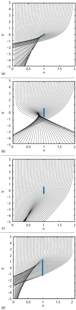
Figure 32 Deflection of trajectories of parallel light rays coming from infinity. CI = 10 and L >> l (a) CI = 10 and L = 0.5l (b) CI = 10 and L = l (c) and CI =1 and L = 10l (d).54
As shown in Figure 26, the Möbius effect enables energy harvesting (energy is not lost at each stage but re-circulates in closed path). While the benefits of Möbius connected wave-based oscillators are evident, this topology still has a limited tuning range of 10 to 20 percent. In this article, a novel approach for improving the tuning range is suggested and validated with the practical example of a 4 to 12 GHz/12 to 18 GHz oscillator based on a metamaterial Möbius strips resonator.
The phase-injections (perturbations) at different nodal points on the strips improve the tuning-range and phase noise performance of Möbius strip based frequency-generating circuits. The oscillator circuit shown in Figure 27 works with a DC bias of 5 V and 35 mA; measured output power is typically 0dBm over the operating frequency band. The measured phase noise performance for a 12-18 GHz VCO is -130 dBc/Hz at 1 MHz frequency offset. It has a 6000 MHz tuning range with a phase noise variation within 3-5 dB over the operating frequency band.
The novel negative index Möbius oscillator (NIMO) circuit shown in Figure 28 is built on an 8-mil thick substrate and uses a BFP740 SiGeHBT transistor for providing negative resistance to compensate the losses of the resonator tank. The total DC power consumption is 680 mW (8 V at 85mA), including the buffer amplifier.
Figure 28 shows the typical schematic of 28.5 GHz NIMO circuit that uses a NIMS resonator as a tank network for improving evanescent mode coupled energy of the resonator tank module and a coupled SRR for mode locking and unwanted mode suppression. Figure 29 shows the measured phase noise of -144dBc/Hz at 100 kHz offset with 10.56 dBm output power. The measured FOM at 1MHz is -226 dBc/Hz for 680 mW DC power consumption. The main drawback of this configuration is limited tuning (<5 percent) to compensate for frequency drift due to temperature.
For practical applications, the tuning range must be improved. The tuning capability of the NIMO circuit in Figure 28 is enhanced by incorporating phase-stabilization (manipulating the phase velocity by introducing a mode-suppression ring that allows multi-mode-phase-injection into the Mobius strips cavity). This introduces a Q-multiplier effect and an exponential rise in the Q-factor over the desired tuning range. Table I shows several recently published papers to compare with this work based on FOM.
Wireless and Wearable Electronics
Wireless and wearable implantable biomedical electronics are promising for the continuous real-time measurement of underlying physiological signals such as in electrocardiography,43 electromyography,44 and brain action potentials.45 In these biomedical devices, wireless power and data telemetry are employed to prolong operational life with communication based on backscattering, which can run either without a battery or with just a single rechargeable battery.
Magneto-inductive telemetry is widely used in these devices for wireless power and data transfer. The typical inductive telemetry core consists of a pair of antenna/coils placed coaxially in space, one inside the device and one placed externally as part of the reader/interrogator. The external coil typically transmits data which is also harvested for its power and regulated to power up the implant circuitry. The antennas used for these telemetry systems are either loop wire coils or printed spiral coils. One of the most important design criteria is to maximize the coupling coefficient between external and implanted coils, which affects the power/data transfer efficiency significantly.
There has recently been an effort to use a metamaterial resonator for improved wireless energy transfer. Metamaterial resonators such as SRRs can exhibit strong magnetic resonance to EM waves,46 with high Q factors. This makes them excellent candidates for near-field resonant power/data transfer. The SRR also enables sub-wavelength focusing of the incident energy at resonance in the capacitive gap of the metamaterial, which could be harvested for energy/power. Compared to a conventional antenna/coil system for power telemetry, the SRR provides a compact and low profile geometry due to an integrated antenna and resonator function built into the structure. 47
Coupled mode theory (CMT)48 predicts that when the resonances of both coils are matched, within the “strongly coupled regime,” it results in maximal energy transfer between the coils. However, if the resonance of either of the coils deviates from one another, the power transfer efficiency drops sharply. Since the biological environment is expected to vary due to physiological changes, it is very hard to match their resonances. This issue is especially critical for metamaterial-based energy harvesters49-50 due to their sharp narrowband resonances, thus automatic tuning of resonances is necessary. This can be done for conventional coils with tunable varactors;51-52 however, the tuning needs precision, adds complexity in the system and may be difficult with motion artifacts. The alternative is to embed of non-foster impedance circuitry inside the SRR metamaterial to achieve optimal power transfer over a broad band without the need for any tuning.
Current wireless power transfer (WPT) technology allows power transfer only over a limited distance because, as the distance between the transmitter (Tx) and receiver (Rx) coils increases, the power transfer efficiency (PTE) decreases with a steep slope, while the electromagnetic field (EMF) leakage increases. In order to increase PTE and decrease EMF leakage simultaneously, we need a method to concentrate the magnetic fields between the Tx and Rx coils. In this article, we proposed a novel metamaterial structure to realize high efficiency and low EMF leakage. Metamaterial can confine the magnetic fields between the Tx and Rx coils by negative relative permeability, including the reduction in leakage. Figure 30 shows a typical experimental setup for optimized efficiency of wireless power transfer.53
Artificial Gravitational Field
The generation of artificial gravitational fields with electric currents could in principle be detected through the induced change in space-time geometry that results in a purely classical deflexion of light by magnetic fields. Fuzfa 54 has proposed the experimental set-up shown in Figure 31 that includes stacked large superconducting Helmholtz coils for the generation of the artificial gravitational field and the detection would be achieved by highly sensitive Michelson interferometers whose arms contain Fabry-Perot cavities to store light into the generated gravitational field. As depicted in Figure 31, the amplitude of the phase shift accumulated during the bouncing of light in the curved space-time generated by the magnetic field would reach, in a few months, the level of an astrophysical source of gravitational wave passing through ground-based GW observatories.55 Since space-time is slightly shrunk inside the superconducting coils, light trapped inside the powered coil accumulates phase shift as round trips succeed each other. The sensitivity and dynamic range of superconducting coils can be increased by incorporating MMI superconducting coils. The ongoing research in the MMI field could open new eras in experimental gravity and laboratory tests of space-time bends based on equivalence principle of general theory of relativity.
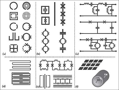
Figure 33 Typical symbolic representation of a superconducting metamaterial as a subset of meta-atoms and meta-molecules: magnetically active meta-atoms (a) electrically active meta-atoms (b) transmission line metamaterials (c) lumped element meta-atoms (d) various meta-molecule realizations (e) and DC magnetic cloak structures (f).57
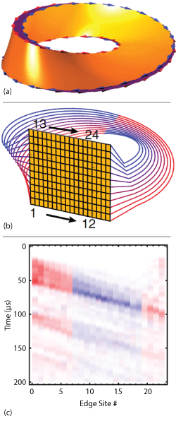
Figure 34 Typical topological Möbius metamaterial insulator: Möbius TI, with the arrow indicating the edge propagation direction, color the spin state (a) connectivity of the Möbius TI, with metamaterial PCB and external connections generating the topology indicating spin on traversing the edge (b) and spin-resolved detection of edge transport after excitation of ↑. ↑ and ↓ intensities are plotted in the red and blue channels, respectively, showing the conversion from ↑ to ↓ when the excitation moves from one edge to the other (c).
Figure 32 illustrates the deflected trajectories of a bundle of rays of incoming parallel light from spatial infinity, these trajectories have been obtained from the numerical resolution of geodesic equations in strongly curved space-times around a loop of solenoids with extremely large magneto-gravitational coupling (CI) so that the way light is deflected can be easily shown. Deflections of trajectories are plotted with different values of solenoid length (L), radius of current loop (l) and magneto-gravitational coupling (CI) strength.54
MMI structures represent artificially engineered materials that can create and enable unique interactions of matter with electromagnetic and gravitational waves.
MMI Superconducting Coils
Superconductors offer unique advantages compared to ordinary metal, semiconductor and dielectric meta-atoms, namely: low loss, flux quantization and Josephson effects, quantum interactions between photons and discrete energy states in the meta-atom, and strong diamagnetism.56
Figure 33 shows the typical symbolic representation of a superconducting metamaterial as a subset of meta-atoms and meta-molecules. Superconducting quantum metamaterial opens the possibility to explore collective quantum dynamics under very strong coupling between electromagnetic fields, gravitational field and artificial atoms.57
Metamaterial, where interaction strengths and length scales can be engineered, are a promising avenue for studying topological structure such as Möbius strips. Time-reversal broken topological metamaterial have been realized in the microwave domain via a lattice of chiral magnetic (gyrotropic) resonators.58-59 Figure 34 shows a typical Möbius metamaterial insulator, realized by connecting the left and right edges of the system with a half twist and a spin flip.60
As illustrated in Figure 34b, “a” inductor j sites from the top of the left edge are connected to the “b” inductor at the j sites from the bottom of the right edge. The spin flip is necessary, as “up” spins propagate rightwards on the top edge but leftwards on the bottom edge.61 Figure 34b shows the temporal dynamics of a spin-up excitation in the system; it propagates rightward along the system edge, until it reaches the other edge, is converted into a down spin, and continues its progression around the system perimeter; this cycle is repeated until the excitation is damped out by the finite system Q.
Conclusion
Part 2 discusses MMS resonator based topology that enables next generation energy efficient signal source solutions in integrated circuit and surface mounted planar technology. The unique features of Möbius metamaterial strips promise many future inventions, recurring in an endless loop – one could say that the future exists on a Möbius strips surface. Part 3 will follow in the July 2016 issue.
References
- D. R. Smith, S. Schultz, P. Markos and C. M. Soukoulis, “Determination of Effective Permittivity and Permeability of Metamaterials from Reflection and Transmission Coefficients,” Physical Review B, Vol. 65, No. 19, April 2002, pp. 195104-1-5.
- D. R. Smith, D. C. Vier, T. Koschny, and C. M. Soukoulis, “Electromagnetic Parameter Retrieval from Inhomogeneous Metamaterials,” Physical Review E, Vol. 71, No. 3, March 2005, pp. 36617-1-11.
- U. C. Hasar and J. J. Barroso, “Retrieval Approach for Determination of Forward and Backward Wave Impedances of Bianisotropic Metamaterials,” Progress In Electromagnetics Research, Vol. 112, 2011, pp. 109–124.
- J. B. Pendry, A. J. Holden, D. J. Robbins and W. J. Stewart, “Low Frequency Plasmons in Thin-Wire Structures,” Journal of Physics: Condensed Matter, Vol. 10, No. 22, June 1998, pp. 4785–4809.
- R. Marqués, F. Medina and R. Rafii-El-Idrissi, “Role of Bianisotropic in Negative Permeability and Left-Handed Metamaterials,” Physical Review B, Vol. 65, No. 14, April 2002, pp. 144440-1-6.
- A. M. Nicolson and G. Ross, “Measurement of the Intrinsic Properties of Materials by Time-Domain Techniques,” IEEE Transactions on Instrumentation and Measurement, Vol. 19, No. 4, November 1970, pp. 377–382.
- W. B. Weir, “Automatic Measurement of Complex Dielectric Constant and Permeability at Microwave Frequencies,” Proceedings of the IEEE, Vol. 62, No. 1, January 1974, pp. 33–36.
- V. Milosevic, B. Jokanovic and R. Bojanic, “Effective Electromagnetic Parameters of Metamaterial Transmission Line Loaded With Asymmetric Unit Cells,” IEEE Transactions on Microwave Theory and Techniques, Vol. 61, No. 8, August 2013, pp. 2761–2772.
- L.D. Landau, L. P. Pitaevskii and E.M. Lifshitz, Electrodynamics of Continuous Media, 2nd ed. Oxford, U.K.: Pergamon, 1984.
- J. W. Graham, "Arbitrary Oriented Biaxial Anisotropic Media: Wave Behaviors and Microstrip Antennas," Ph.D. Dissertation, Syracuse University, May 2012.
- T. Koschny, P. Markoš, E. N. Economou, D. R. Smith, D. C. Vier, and C. M. Soukoulis, “Impact of Inherent Periodic Structure on Effective Medium Description of Left-Handed and Related Metamaterials,” Physical Review B: Condensed Matter, Vol. 71, No. 24, June 2005, pp. 245105-1-22.
- A. Alù, “Restoring the Physical Meaning of Metamaterial Constitutive Parameters,” Physical Review B, Condensed Matter, Vol. 83, No. 8, February 2011, pp. 081102-1-4.
- L. Chen, Z. -Y. Lei, R. Yang, X. -W. Shi and J. Zhang, “Determining the Effective Electromagnetic Parameters of Bianisotropic Metamaterials with Periodic Structures,” Progress In Electromagnetics Research M, Vol. 29, 2013, pp. 79–93.
- X. Chen, T. M. Grzegorczyk, B. -I Wu, J. Pacheco, Jr. and J. A. Kong, “Robust Method to Retrieve the Constitutive Effective Parameters of Metamaterial,” Physical Review E, Vol. 70, No. 1, July 2004, pp. 16608-1-7.
- U. L. Rohde and A. K. Poddar, “Möbius Metamaterial Inspired Next Generation Circuits and Systems,” Microwave Journal, Vol. 59, No. 5, May 2016.
- X. Chen, B. -I. Wu, J. A. Kong and T. M. Grzegorczyk, “Retrieval of the Effective Constitutive Parameters of Bianisotropic Metamaterial,” Physical Review E, Vol. 71, No. 4, April 2005, pp. 046610.
- R. Marqués, F. Martín, M. Sorolla, Metamaterial with Negative Parameters: Theory, Design and Microwave Applications, Wiley, 2008.
- O. Sydoruk1, E. Tatartschuk1, E. Shamoninal and L. Solymar, “Analytical Formulation for the Resonant Frequency of Split Rings,” Journal of Applied Physics, Vol. 105, No. 1, January 2009, pp. 14903.
- X. Chen, T. M. Grzegorczyk and J. A. Kong, “Optimization Approach to the Retrieval of the Constitutive Parameters of a Slab of General Bianisotropic Medium,” Progress In Electromagnetics Research, Vol. 60, 2006, pp. 1–18.
- Z. Li, K. Aydin and E. Ozbay, “Determination of the Effective Constitutive Parameters of Bianisotropic Metamaterials from Reflection and Transmission Coefficients,” Physical Review E, Vol. 79, No. 2, February 2009, pp. 026610-1-7.
- U. C. Hasar, “Procedure for Accurate and Stable Constitutive Parameters Extraction of Materials at Microwave Frequencies,” Progress In Electromagnetics Research, Vol. 109, 2010, pp. 107–121.
- J. Wang, S. Qu, J. Zhang, H. Ma, Y. Yang, C. Gu and X. Wu, “A Tunable Left-Handed Metamaterial Based on Modified Broadside-Coupling Split-Ring Resonators,” Progress In Electromagnetics ResearchLetters, Vol. 6, 2009, pp. 35-45.
- T. Nakamura, T. Masuda, N. Shiramizu, A. Nakamura and K. Washio, “A 11.1-V Regulator-Stabilized 21.4-GHz VCO and a 11.5% Frequency-Range Dynamic Divider for K-Band Wireless Communication,” MTT-Transactions,Vol. 60, No. 9, September 2012, pp. 2823–2832.
- Z. Chen, W. Hong, J. Chen and J. Zhou, “Design of High-Q Tunable SIW Resonator and its Application to Low Phase Noise VCO,” IEEE Microwave and Wireless Components Letters, Vol. 23, No. 1, January 2013, pp. 43–45.
- A. Collado, F. Mira and A. Georgiadis, “Mechanically Tunable Substrate Integrated Waveguide (SIW) Cavity Based Oscillator,” IEEE Microwave and Wireless Components Letters, Vol. 23, No. 9, September 2013, pp. 489-491.
- C. -L. Chang, C. -H. Tseng and H. -Y. Chang, “A New Monolithic Ka-Band Filter-Based Voltage Controlled Oscillator Using 0.15um GaAs PHEMT Technology,” IEEE Microwave and Wireless Components Letters, Vol. 24, No. 2, February 2014, pp. 111–113.
- Y. Chen, K. Mouthaan and F. Lin “Design of X-band and Ka-band Colpitts oscillators Using a Parasitic Cancellation Technique,” IEEE Transactions on Circuits and Systems-I, Vol. 57, No. 8, August 2010, pp. 1817–1828.
- Ulrich L. Rohde and Ajay K. Poddar, “Möbius Metamaterial Inspired Next Generation Circuits and Systems,” Microwave Journal, Vol. 59, No. 5, May 2016.
- A. Poddar, Slow Wave Resonator Based Tunable Multi-Band Multi-Mode Injection-Locked Oscillator, Habil Thesis, BTU Cottbus, Germany, 2014.
- S. A. Marvel, R. E. Mirollo and S. H. Strogatz, “Identical Phase Oscillators with Global Sinusoidal Coupling Evolve by Möbius Group Action,” Chaos: An Interdisciplinary Journal of Nonlinear Science, Vol. 19, No. 4, December 2009, pp. 043104-1-4.
- E. Martens, “Cooperative Behavior in Networks of Coupled Oscillators,”Ph.D. Diss., Faculty of the Grad School of Cornell University, May 2009.
- A. Rofougaran, J. Rael, M. Rofougaran and A. Abidi, “A 900 MHz CMOS LC Oscillator with Quadrature Outputs,” IEEE International Solid State Circuits Conference Digest, February 1996, pp. 392–393.
- L. Guansheng, E. Afshari, “A Low Phase Noise Multi-Phase Oscillator Based on Left-Handed LC-Ring,” IEEE Journal of Solid State Circuits, Vol. 45, No. 9, September 2010, pp. 1822–1833.
- L. Romano, A. Bonfanti, S. Levantino, C. Samori and A. L. Lacaita, “5-GHz Oscillator Array with Reduced Flicker Up-Conversion in 0.13-um CMOS,”IEEE Journal of Solid State Circuits, Vol. 41, No. 11, November 2006, pp. 2457–2467.
- J. Wood, T. C. Edwards and Steve Lipa, “Rotary Travelling-Wave Oscillator Arrays: a New Clock Technology,” IEEE Journal of Solid State Circuits, Vol. 36, No. 11, November 2001, pp. 1654–1665.
- H.T. Ahn and D. J. Allstot, “A 0.5-8.5-GHz Fully Differential CMOS Distributed Amplifier,” IEEE Journal of Solid State Circuits, Vol. 37, No. 8, August 2002, pp. 985–993.
- D. Ham and W. Andress, “A Circular Standing Wave Oscillator,” IEEE Solid State Circuits Conference Digest, Vol. 1, February 2004, pp. 380–533.
- T. Nakamura, T. Masuda, N. Shiramizu, A. Nakamura and K. Washio, “A 1.1-V Regulator-Stabilized 21.4-GHz VCO and a 11.5% Frequency-Range Dynamic Divider for K-Band wireless communication”, IEEE Transactions on Microwave Theory and Techniques, Vol. 60, No. 9, September 2012, pp. 2823-2832.
- Z. Chen, W. Hong, J. Chen and J. Zhou, “Design of High-Q Tunable SIW Resonator and its Application to Low Phase Noise VCO,” IEEE Microwave and Wireless Components Letters, Vol. 23, No. 1, January 2013, pp. 43–45.
- A. Collado, F. Mira and A. Georgiadis, “Mechanically Tunable Substrate Integrated Waveguide (SIW) Cavity Based Oscillator,” IEEE Microwave and Wireless Components Letters, Vol. 23, No. 9, September 2013, pp. 489–491.
- C. -L. Chang, C. -H. Tseng and H. -Y Chang, “A New Monolithic Ka-Band Filter-Based Voltage Controlled Oscillator Using 0.15um GaAs PHEMT Technology,” IEEE Microwave and Wireless Components Letters, Vol. 24, No. 2, February 2014, pp. 111–113.
- Y. Chen, K. Mouthaan and F. Lin “Design of X-Band and Ka-Band Colpitts Oscillators Using a Parasitic Cancellation Technique,” IEEE Transactions on Circuits and Systems-I, Vol. 57, No. 8, August 2010, pp. 1817–1828.
- J. Riistama, E. Aittokallio, J. Verho and J. Lekkala, “Totally Passive Wireless Biopotential Measurement Sensor by Utilizing Inductively Coupled Resonance Circuits,” Sensors and Actuators A: Physical, Vol. 157, No. 2, February 2010, pp. 313-321.
- D. J. Young, “Wireless Powering and Data Telemetry for Biomedical Implants,” International Conference of the IEEE Engineering in Medicine and Biology Society, September 2009, pp. 3221–3224.
- W. Biederman, D. J. Yeager, N. Narevsky, A. C. Koralek, J. M. Carmena, E. Alon and J. M. Rabaey, “A Fully-Integrated, Miniaturized (0.125 mm²) 10.5 µW Wireless Neural Sensor Solid-State Circuits,” IEEE Journal of Solid State Circuits, Vol. 48, No. 4, April 2013, pp. 960–970.
- V. G. Veselago, “The Electrodynamics of Substances with Simultaneously Negative Values of εand µ,” Sov Phys Uspekhi, Vol. 10, No. 4, 1968, pp. 509–514.
- R. A. Shelby, D. R. Smith and S. Schultz, “Experimental Verification of a Negative Index of Refraction,” Science, Vol. 292, No. 5514, April 2001, pp. 77-79.
- A. Kurs, A. Karalis, R. Moffatt, J. D. Joannopoulos, P. Fisher and M. Soljacˇic´, “Wireless Power Transfer via Strongly Coupled Magnetic Resonances,” Science, Vol. 317, No. 5834, July 2007, pp. 83–86.
- A. M. Hawkes, A. R. Katko S. A. Cummer, “A Microwave Metamaterial with Integrated Power Harvesting Functionality,” Applied Physics Letters, Vol. 103, No. 16, October 2013, p. 163901.
- O. M. Ramahi, T. S. Almoneef, M. Alshareef and M. S. Boybay, “Metamaterial Particles for Electromagnetic Energy Harvesting,” Applied Physics Letters, Vol. 101, No. 17, October 2012, p. 173903.
- J. M. Wilson, R. Bashirullah, D. P. Nackashi, D. A. Winick, B. E. Duewer and P. D. Franzon, “Design of Rotating MEMS Tunable Capacitors for use at RF and Microwave Frequencies,” Proceedings of the SPIE, Vol. 4593, 2001, pp. 186–197.
- A. S. Y. Poon and M. Taghivand, “Supporting and Enabling Circuits for Antenna Arrays in Wireless Communications,” Proceedings of the IEEE, Vol. 100, No. 7, July 2012, 2207–2218.
- Y. Cho, J. J. Kim, D. -H. Kim, S. Lee, H. Kim, C. Song, S. Kong, H. Kim, C. Seo, S. Ahn and J. Kim, “Thin PCB-Type Metamaterial for Improved Efficiency and Reduced EMF Leakage in Wireless Power Transfer Systems,” IEEE Transactions on Microwave Theory and Techniques, Vol. 64, No. 2, February, 2016 pp. 353-364.
- A. Fuzfa, “How Current Loops and Solenoids Curve Space-Time,” Physical Review D, V3, December 2015.
- W. Chaibi, R. Geiger, B. Canuel, A. Bertoldi, A. Landragin and P. Bouyer, “Low Frequency Gravitational Wave Detection With Ground Based Atom Interferometer Arrays,” Physical Review D, January 2016.
- S. M. Anlage, “The Physics and Applications of Superconducting Metamaterials,” Journal of Optics, Vol. 13, No. 2, April 2010.
- P. Jung, A. V. Ustinov and S. M. Anlage, “Progress in Superconducting Metamaterials,” Superconductor Science Technology, Vol. 27, May 2014.
- Z. Wang, Y. D. Chong, J. D. Joannopoulos and M. SoljaSoljacˇic´, “Reflection-Free One-Way Edge Modes in a Gyromagnetic Photonic Crystal,” Physical Review Letters, Vol. 100, No. 1, February 2008.
- Z. Wang, Y. Chong, J. D. Joannopoulos and M. Soljacic, “Observation of Unidirectional Backscattering-Immune Topological Electromagnetic States,” Vol. 461, No. 7265, October 2009, pp. 772–775.
- J. Ningyuan, C. Owens, A. Sommer, D. Schuster and J. Simon, “Time- and Site-Resolved Dynamics in a Topological Circuit,” American Physical Society, Vol. 5, No. 2, June 2015.
- L. T. Huang and D. H. Lee, “Topological Insulators on a Mobius Strip,” Physical Review B, Vol. 84, No. 19, November 2011.