
 | |||
| Fig. 1 IEEE 802.11 WLAN frequency allocations. t | |||
Due to the rapidly growing demand for broadband wireless communication, the operating frequency is moving toward the 5 GHz U-NII band. With a maximum data rate of 54 Mb/s, the IEEE 802.11a wireless LAN (WLAN) standard specifies 300 MHz allocation of spectrum in the 5 GHz band that is divided into three sub-bands, as shown in Figure 1.1,2 The lower and middle U-NII sub-bands from 5.15 to 5.35 GHz accommodate eight channels in a total bandwidth of 200 MHz. The 100 MHz bandwidth of the upper U-NII band, from 5.725 to 5.825 GHz, accommodates four channels. The IEEE 802.11b/g WLAN standard specifies an 83 MHz allocation of spectrum in the 2.4 GHz ISM band (from 2.4 to 2.483 GHz), which has a great advantage in that it is accepted worldwide. The 802.11b (Wi-Fi) has a nominal maximum data rate of 11 Mb/s. The 802.11g provides a 54 Mb/s capability in a 2.4 GHz environment by using the technically advanced orthogonal frequency division multiplexing (OFDM) modulation scheme that 802.11a uses, while also supporting the same direct-sequence spread-spectrum (DSSS) modulation scheme as 802.11b. A 2.4/5.7 GHz dual-band WLAN system, which supports both 802.11a and 802.11b/g, will be desired for future WLAN applications.
To implement a 2.4/5.7 GHz dual-band WLAN receiver, a direct conversion receiver (DCR) is more suitable for integrated circuit design than a heterodyne receiver, since an external image-reject filter is no longer required. As shown in Figure 2, the received RF signal is selected by a filter, amplified by a low noise amplifier and down-converted to baseband by an I/Q mixer. A direct conversion receiver suffers from more serious DC-offset effect, flicker noise and I/Q imbalance than an heterodyne receiver. However, in the 802.11a/g system, there is a 312.5 kHz empty region around zero frequency, and the DC-offset and flicker noise is less sensitive. Without loss of information, the DC offset can be removed by a high pass filter with a corner frequency less than 156 kHz.3 Hence, the DCR architecture is still an attractive choice for a 802.11a/g WLAN system.
 | ||
| Fig. 2 Architecture of a 2.4/5.7 GHz concurrent dual-band direct-conversion receiver. | ||
Dual-band LNA Circuit Design
The LNA design considerations include linearity, stability, noise figure, input/output match and DC bias. For the low power consumption requirement, a low DC current is expected. In CMOS LNA design, the most important procedure is to choose the right NMOS transistor channel width, which has the lowest noise figure.4 Here, the single-band LNA design procedure will be introduced first. It is then extended to design the concurrent dual-band LNA.
Design Procedure for a Single-band LNA
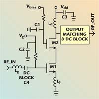
As shown in Figure 3, there are several steps in the design of a cascode CMOS LNA:
 | |||
| Fig. 3 Circuit schematic of a cascode CMOS LNA. | |||
1. The cascode configuration of an LNA can achieve better frequency response and stability.
2. According to Shaeffer and Lee,4 the sources of noise and how to choose the gate width of the first stage transistor can be determined. A reasonable current consumption can be set and then the transistor channel width of M1 is chosen from the noise figure optimization procedure. To meet the power consumption limit, the chosen gate width of the first stage transistor M1 is 120 µm (48 x 2.5 µm). A multi-finger layout technology is used to reduce the noise from the transistor gate resistance.
3. The gate width of the second stage is chosen to be half that of the first stage. Too large a gate width leads to an unstable circuit.
4. To achieve an input match to the 50 Ω characteristic impedance of the system, a series off-chip inductance Lg, a DC block capacitance C4, the parasitic capacitor Cgs and the bondwire equivalent inductance Ls are used. The bond-wire equivalent inductance Ls is used to match the real part of the input impedance to the characteristic impedance. The combination of gate and source bond-wire equivalent inductances cancels the reactance of the parasitic capacitance Cgs at the resonant frequency (w0) of the input transistor M1. The expression for the input impedance Zin is4
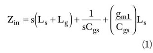
At the resonant frequency,

where

5. The on-chip inductance Ld is used for the cascode stage inductive load so that its resonant frequency is close to the operating frequency range. The choice of an inductive load has another advantage — no extra DC voltage drop. The parallel resonant frequency of the inductance Ld and the parasitic capacitance of M2 is designed to be close to the operating frequency. The series capacitance and inductance perform the output matching to the characteristic impedance of the system.
6. In a single-ended circuit design, bypass capacitors are important. C1 provides an AC ground to the common gate stage and C3 provides an AC ground to assure that the parallel resonance will not be affected by other parasitics, such as bond-wires, test board microstrip line effects and supply noises. Once the components are combined, the LNA is analyzed to assure that it is unconditionally stable from DC to 10 GHz.
Design Procedure for the Concurrent Dual-band LNA
The circuit schematic and RFIC layout of a 2.4/5.7 GHz concurrent dual-band CMOS cascode LNA are shown in Figure 4. When the DC operating point is determined, the most important procedure is to choose the optimal NMOS transistor channel-width that has the lowest noise figure. The gate-to-source capacitance (Cgs) can then be derived. The chosen gate width of the first-stage transistor M1 is 120 µm. For the input impedance to be 50 Ω at 2.4 and 5.7 GHz, a parallel LC network (which suppresses the unwanted frequency band signal) is connected in series with the DC block capacitor C4 and the inductance of Lg. The Zg resonates with Cgs at both frequency bands of interest. A metal-insulator-metal (MIM) capacitor and an on-chip spiral inductor are used. The output-matching network consists of an added series LC branch in parallel with the parallel tank of a single-band LNA.5-6 The series LC branch determines the frequency of the notch in the gain transfer function of the LNA.
 | ||
| Fig. 4 A 2.4/5.7 GHz concurrent dual-band CMOS LNA’s (a) schematic and (b) RFIC layout. | ||
Simulated and Measured Results
The Agilent Advance Design System (ADS) is used for design simulation. The circuit measurement is performed with an on-wafer test set-up. Simulation and measured S-parameter results are shown in Figure 5. It can be observed that the measured input-matching response is shifted to a higher frequency (especially for the 5.7 GHz band), compared with the simulation results. Consequently, the dual-band LNA performance will show a certain degree of degradation.
 | ||
| Fig. 5 Simulated and measured S-parameters of the concurrent dual-band LNA. | ||
Figures 6 and 7 show the LNA’s measured noise figure and gain, respectively. The LNA at 2.44 GHz exhibits a linear (power) gain of 7.6 dB, a noise figure of 5.7 dB, an input return loss of 9.5 dB, an output return loss of 2.7 dB, a P1dB of –9.3 dBm and an IIP3 of –1.5 dBm. At 5.76 GHz, it has a linear (power) gain of 8.6 dB, a noise figure of 6.8 dB, an input return loss of 6.2 dB, an output return loss of 11.2 dB, a P1dB of –10 dBm and an IIP3 of –2.4 dBm.
 | ||
| Fig. 6 Measured noise figure of a concurrent dual-band CMOS LNA. | ||
 | ||
| Fig. 7 Measured input P1dB of a concurrent dual-band CMOS LNA at (a) 2.44 and (b) 5.76 GHz. | ||
 | |||
| Fig. 8 Two-tone test of a concurrent dual-band CMOS LNA at (a) 2.44 GHz, IIP3 = -1.5 dBm and (b) 5.76 GHz, IIP3 = -2.4 dBm. | |||
 | |||
| Fig. 9 A concurrent dual-band CMOS LNA’s (a) chip micrograph and (b) test set-up. | |||
Figure 8 shows the results of a two-tone IMD test. The power consumption of the concurrent dual-band LNA is 10.8 mW at VDD = 1.8 V. Although a much better performance of the dual-band CMOS LNA has been reported by Hashemi and Hajimiri,5-6 it was achieved by using massive off-chip matching networks. In this fully-integrated CMOS LNA design, all on-chip matching elements are used. Hence, due to the lower Q values and the CMOS process variations (about ±10 percent) for the on-chip matching elements, further study will be needed to achieve the same performance level as reported in Hashemi and Hajimiri.5–6
Figure 9 shows the chip micrograph and a photograph of an on-wafer microwave probe-station measurement set-up for the 2.4/5.7 GHz concurrent dual-band CMOS LNA. The chip size is 1.076 by 1.072 mm. Table 1 summarizes the simulated and measured performance of the designed concurrent dual-band LNA.
 | ||
Conclusion
This article presents the design of a fully-integrated 2.4/5.7 GHz concurrent dual-band LNA for 802.11 WLAN DCR applications. The dual-band LNA is fabricated in a TSMC 0.18 µm 1P6M standard CMOS process. The chip size is 1.076 by 1.072 mm. It simultaneously provides narrow-band gain and matching at both the 2.4 and 5.7 GHz bands. The measurement is performed using an on-wafer test set-up. The dual-band LNA measurements at 2.44/5.76 GHz exhibit a linear (power) gain of 7.6/8.6 dB, a noise figure of 5.7/6.8 dB, an input return loss of 9.5/6.2 dB, an output return loss of 2.7/11.2 dB, a P1dB of –9.3/–10 dBm and an IIP3 of –1.5/–2.4 dBm. The power consumption of the concurrent dual-band LNA is 10.8 mW at VDD = 1.8 V. In this fully-integrated dual-band LNA design, due to the lower Q values and the CMOS process variation (about ±10 percent) for the on-chip matching elements, further study will be necessary to achieve the same performance level listed in other reports, which use massive off-chip matching networks.
Acknowledgment
The authors would like to thank the Chip Implementation Center (CIC) of the National Science Council, Taiwan, ROC, for its support of the TSMC CMOS process.
References
- IEEE standard 802.11a: High Speed Physical Layer in the 5 GHz Band.
- R. van Nee and R. Prasad, OFDM Wireless Multimedia Communication, Artech House Inc., Norwood, MA 2000.
- B. Razavi, “A 2.4 GHz CMOS Receiver for IEEE 802.11 Wireless LANs,” IEEE Journal of Solid-State Circuits, Vol. 34, No. 10, October 1999, pp. 1382–1385.
- D.K. Shaeffer and T.H. Lee, “A 1.5 V 1.5 GHz CMOS Low Noise Amplifier,” IEEE Journal of Solid-State Circuits, Vol. 32, No. 5, May 1997, pp. 745–759.
- H. Hashemi and A. Hajimiri, “Concurrent Dual-band CMOS Low Noise Amplifiers and Receiver Architectures,” 2001 Symposium on VLSI Circuits, Digest of Technical Papers, 22-3, pp. 247–250.
- H. Hashemi and A. Hajimiri, “Concurrent Multiband Low Noise Amplifiers – Theory, Design and Applications,” IEEE Transaction on Microwave Theory and Techniques, Vol. 50, No. 1, January 2002, pp. 288–301.
- T.H. Lee, The Design of CMOS Radio-frequency Integrated Circuits, Cambridge University Press, New York, NY 1998.
- B. Razavi, RF Microelectronics, Prentice Hall, 1997.
Qiu-Huan Huang received his MSEE degree from National Cheng Kung University, Tainan, Taiwan, in 2003, where he studied 2.4 GHz CMOS receiver RFICs. He is currently with Ali Corp. as an R&D engineer. His research interests include RFIC and analog IC designs for wireless communication systems.
Dar-Ron Huang received his BSEE degree from National Cheng Kung University, Tainan, Taiwan, in 2002. He is currently working toward his master’s degree. His research interests include RFIC/MMIC designs for wireless communication systems.
Huey-Ru Chuang received his BSEE and MSEE degrees from National Taiwan University, Taipei, Taiwan, in 1977 and 1980, respectively, and his PhD degree in electrical engineering from Michigan State University, East Lansing, MI, in 1987. From 1987 to 1988, he was a post-doctoral research associate at the Engineering Research Center, Michigan State University. From 1988 to 1990, he was with the Portable Communication Division of Motorola Inc., Ft. Lauderdale, FL. He joined the department of electrical engineering at National Cheng Kung University, Tainan, Taiwan, in 1991, where he is currently a professor. His research interests include antenna and RFIC/microwave circuits design for wireless communications, computational electromagnetics and applications, EMI/EMC, microwave communication and detection systems.