
In this work, the basic characteristics of the comb-type capacitive transmission line (CCTL) structure were investigated for application to the development of miniaturized on-chip passive components. According to the results, the CCTL structure showed short wavelength characteristics, due to its periodically added capacitance. The wavelength of the CCTL structure was only 10 percent of that of a conventional microstrip line on a MMIC. The CCTL structure showed a propagation constant much higher than a conventional microstrip line, due to the slow-wave propagation on a periodic structure. Using the CCTL structure, a highly miniaturized impedance transformer was fabricated on a GaAs MMIC. The impedance transformer showed good RF performances in a broadband from S- to X-Band, and its size was 0.042 mm2, which is 0.95 percent of the size of the transformer fabricated by a conventional microstrip line.
With the evolution of integrated circuit (IC) technology, the demands for on-chip RF passive components on ICs have increased in the wireless communication systems market.1-8 However, bulky RF passive components, such as conventional impedance transformers and dividers, have been fabricated outside of the ICs, due to their large sizes. According to a previous report,5 of all the slow-wave structures,3-8 the CCTL structure showed the shortest wavelength. For application to various on-chip components on a MMIC, the basic characteristics of the CCTL structure should be explored thoroughly. In this work, using theoretical and experimental analyses, the basic characteristics of the short wavelength CCTL structure on a GaAs MMIC were investigated to the development of miniaturized on-chip passive components. In addition, using the CCTL structure, a highly miniaturized on-chip passive component was fabricated on a GaAs MMIC.
Basic Characteristics of CCTL
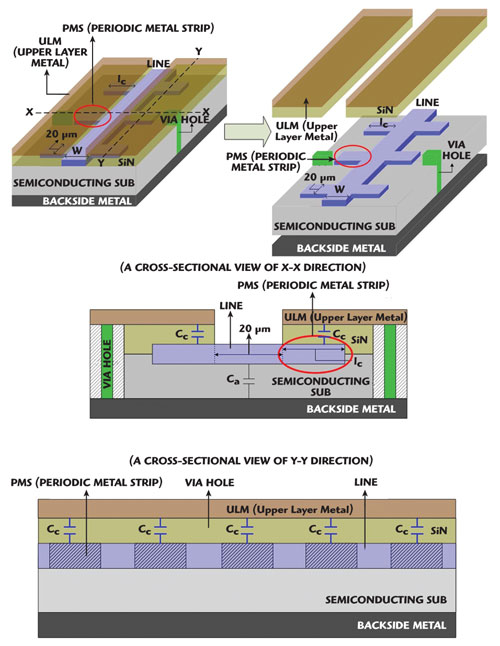
Figure 1 Structure of a CCTL.
Figure 1 shows the structure of a CCTL.5 As shown, a comb-type line is fabricated on the semiconducting substrate. The comb-type line consists of a line and periodic metal strips (PMS), which are connected to both sides of the line. The upper layer metal (ULM) is placed on the top side of the CCTL structure and is electrically connected to the backside ground plane through the via-holes. Therefore, the ULM serves as a ground plane, together with the backside ground plane. A SiN film is deposited between the ULM and PMS for tight coupling. As is well known, a conventional microstrip line has only a periodic capacitance Ca (shown in Figure 1) between the line and the backside ground plane, while the CCTL structure has an additional capacitance Cc as well as Ca, due to a strong electromagnetic coupling between PMS and ULM. Therefore, the CCTL structure exhibits a much shorter wavelength (λg) than conventional ones, because λg is inversely proportional to the periodic capacitance; in other words, λg = 1/[f (LC)0.5].
Short Wavelength Characteristics of CCTL
Figure 2 shows a comparison of the wavelength for CCTL and a conventional transmission line. The spacing L between the strips and the line width, W, which are shown in Figure 1, are all 20 μm. The length of PMS lc varies from 10 to 30 μm. The CCTL structure was fabricated on a GaAs substrate with a height of 100 mm. Compared with a conventional microstrip line, the wavelength of the CCTL structure is only 10 percent of the one of a conventional microstrip line on a MMIC. In short, at 10 GHz, the wavelengths of the CCTL and the conventional microstrip line are 1.06 and 10.56 mm, respectively.
Characteristic Impedance of CCTL
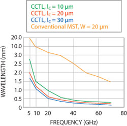
Figure 2 CCTL and conventional microstrip line wavelengths.
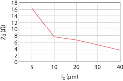
Figure 3 Characteristic impedance of the CCLT.
It can easily be seen that an increase of lc results in an enhancement of the periodic capacitance Cc, due to an increase of the capacitive area. Therefore, the characteristic impedance Z0 of the CCTL can be easily controlled by changing lc, because Z0 depends on the periodic capacitance of the transmission line; in other words, Z0 = (L/C)0.5.9 The dependence of Z0 on lc is shown in Figure 3, where the line width, W, was fixed to a value of 20 μm. The above results indicate that highly miniaturized passive components with various impedances can be realized by using the CCTL structure.
Loss, Propagation Constant and Dielectric Constant
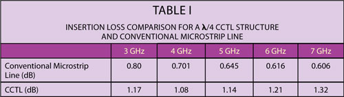
For a fair loss comparison, the loss of a CCTL and a conventional microstrip line with the same electrical length should be compared with each other, because the wavelength of a CCTL structure is much shorter than for a conventional microstrip line. Accordingly, the loss of the CCTL structure and the conventional microstrip line with a length of λ/4 were compared; the results are shown in Table 1. As shown, for an electrical length of λ/4, the CCTL structure shows a little higher loss than the conventional microstrip line. The CCTL structure shows a loss of 1.0 to 1.3 dB, while the conventional microstrip line shows a loss of 0.6 to 0.8 dB. Although the CCTL structure shows a little higher loss, it is preferable for the development of miniaturized passive components on a MMIC, due to its short wavelength.
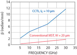
Figure 4 Effective propagation constant of the CCTL structure and conventional microstrip line.
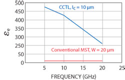
Figure 5 Effective dielectric constant of the CCTL structure and conventional microstrip line.
Figures 4 and 5 show the effective propagation constant and effective dielectric constant of the CCTL structure. As shown, the CCTL structure shows a much higher propagation constant β than the conventional microstrip line, which means that a slow wave exists on CCTL, due to its periodic structure. The effective dielectric constant was obtained from the following equation
As shown, the CCTL structure shows a much higher effective dielectric constant than a conventional microstrip line, due to the slow wave on CCTL.
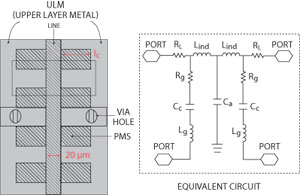
Figure 6 Equivalent circuit of a unit cell of the CCTL structure.
Equivalent Circuit Model of the CCTL Structure on MMIC
For application to the design of RF passive components in a wireless communication system, the equivalent circuit of the CCTL structure should be extracted. Figure 6 shows the equivalent circuit of the unit cell of the CCTL structure, which corresponds to the equivalent circuit of the nth unit section of the periodic structure surrounded by a rectangular box. Cc corresponds to the capacitance between ULM and PMS, which is proportional to the area lh lc, where lh and lc are the width and length of the periodic strips of PMS, respectively, and lh was fixed as 20 μm. Rg and Lg are the resistance and inductance originating from the loss and current flow of the PMS with a length lc. Ca corresponds to the capacitance between line and ground metal. Lind and RL are parasitic inductance and resistance originating from the top line. The capacitances, inductances and resistances of the equivalent circuit are given by
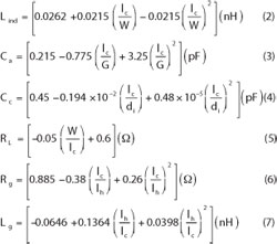
where W, lc and di are top line width, length of periodic metal strip and the thickness of the SiN layer. G is the thickness between line and ground and lh is the width of the PMS. In particular, Equation 4 includes (lc/di)2, because there are nonlinearity originating from parasitics due to the fringing capacitance. Using the equivalent circuit and closed-form equations, the RF characteristics of the CCTL structure were calculated and compared with measured results. Figure 7 shows the measured and calculated insertion loss S21 of the CCTL structure for two lc values. For the calculation results, the equivalent circuit and the closed form equations were used. There is a fairly good agreement between calculated and measured results up to 50 GHz.
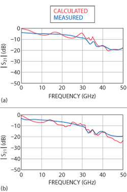
Figure 7 Insertion loss of the CCTL structure (a) lc = 20 µm and (b) lc = 30 µm.
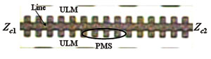
Figure 8 Photograph of the impedance transformer using a CCTL structure.
Highly Miniaturized Impedance Transformer on A GaAs Substrate
A highly miniaturized impedance transformer was fabricated on a GaAs substrate, using the CCTL structure, for application to S- to X-Band MMICs. Figure 8 shows a photograph of the impedance transformer. The characteristic impedance Z0 of the transformer is given by Z0 = (Z c1 Z c2) 0.5 where Zc1 and Zc2 are the source and load impedance, respectively.9 In this work, Zc1 and Zc2 are 12 and 5 Ω, respectively and Z0 is 7.7 Ω. For a Z0 of 7.7 Ω, lc is 10 μm. For a center frequency of 7 GHz, the length of the λ/4 transformer, which was determined from Figure 2, is 0.6 mm, and the line width, W is 70 μm. The size of the transformer employing CCTL is 0.042 mm, which is 0.95 percent of the size of a transformer fabricated using a conventional microstrip line on a MMIC.9 In other words, if λ/4 transformer with a Z0 of 7.7 Ω is fabricated by a conventional microstrip line on a GaAs substrate, the line width, W and a length of λ/4 are 1,170 μm and 3.77 mm, respectively, and its size is 4.41 mm2. Figure 9 shows the measured return loss S11 and insertion loss S21 of the transformer. The insertion and return loss were measured at a port impedance of 50 Ω and was normalized to source and load impedance, Zc1 and Zc2. As shown in this figure, a good transformer RF performance can be observed. The return and insertion loss are 28 and 1.4 dB, respectively, at a center frequency of 7 GHz, and return loss values better than 10 dB and insertion loss values of 1.5 ± 0.5 dB in the 3.2 to 9.2 GHz range.
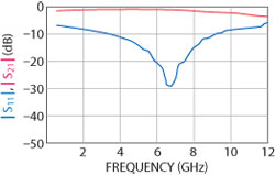
Figure 9 RF characteristics of the impedance transformer using a CCTL structure.
Conclusion
In this work, the basic characteristics of a CCTL structure were investigated for the development of miniaturized on-chip passive components. According to the results, the CCTL structure showed short wavelength characteristics, due to its periodically added capacitance. The wavelength of the CCTL structure was only 10 percent of that of a conventional microstrip line on a MMIC. The CCTL structure showed a propagation constant much higher than a conventional microstrip line, due to the slow wave propagation on the periodic structure. Using the CCTL structure, a highly miniaturized impedance transformer was fabricated on a GaAs MMIC. The impedance transformer showed good RF performances in a broadband from S- to X-Band, and its size was 0.042 mm2, which is 0.95 percent of the size of the transformer fabricated with a conventional microstrip line. The above results mean that the CCTL is a promising candidate for the development of highly miniaturized passive components on a MMIC.
Acknowledgments
This research was supported by the Basic Science Research Program through the National Research Foundation of Korea (NRF), funded by the Ministry of Education, Science and Technology (2010-0007452). This work was financially supported by the Ministry of Knowledge Economy (MKE) and the Korea Industrial Technology Foundation (KOTEF) through the Human Resource Training Project for Strategic Technology. This work was also partly supported by a Grant of the Korean Ministry of Education, Science and Technology (the Regional Core Research Program/Institute of Logistics Information Technology).
References
- A.A. Abidi, “RF-CMOS Comes of Age,” IEEE Journal of Solid State Circuits, Vol. 39, No. 4, April 2004, pp. 840-853.
- J.R. Long, “Passive Components for Silicon RF and MMIC Design,” IEICE Transactions on Electronics, Vol. E86-C, No. 6, June 2003, pp. 1022-1031.
- Y. Yun, J.W. Jung, K.M. Kim, H.C. Kim, W.J. Chang, H.G. Ji and H.K. Ahn, “Experimental Study on Isolation Characteristics Between Adjacent Microstrip Lines Employing Periodically Perforated Ground Metal for Application to Highly Integrated GaAs MMICs,” IEEE Microwave and Wireless Components Letters, Vol. 17, No. 10, October 2007, pp. 703-705.
- Y. Yun, K.S. Lee, C.R. Kim, K.M. Kim and J.W. Jung, “Basic RF Characteristics of the Microstrip Line Employing Periodically Perforated Ground Metal and Its Application to Highly Miniaturized On-Chip Passive Components on GaAs MMIC,” IEEE Transactions on Microwave Theory and Techniques, Vol. 54, No. 10, October 2006, pp. 3805-3817.
- Y. Yun, “A Short Wavelength Comb-Type Capacitive Transmission Line for Application to Miniaturized On-Chip Passive Components on MMIC,” Electronics Letters, Vol. 46, No. 5, March 2010, pp. 352-353.
- D. Ahn, J.S. Park, C.S. Kim, J. Kim, Y. Qian and T. Itoh, “A Design of Low Pass Filter Using the Novel Microstrip Defected Ground Structure,” IEEE Transactions on Microwave Theory and Techniques, Vol. 49, No. 1, January 2001, pp. 86-93.
- A. Lai and T. Itoh, “Microwave Composite Right/Left-handed Metamaterials and Devices,” Proceedings of the 2005 Asia-Pacific Microwave Conference, pp. 31-34.
- J. Gao and L. Zhu, “Per-Unit-Length Parameters of 1-D CPW Metamaterials with Simultaneously Series-C and Shunt-L Loading,” Proceedings of the 2005 Asia-Pacific Microwave Conference, pp. 39-42.
- D.M. Pozar, Microwave Engineering, Addison-Wesley, Reading, MA, 1990.