
In the design of high frequency power amplifiers, the goal is to achieve the power gain and output power at the desired frequency in order to achieve high PAE. Large-signal S-parameters of power devices are normally not provided by the manufacturer. One of the methods to characterize the device is through load- and source-pull. However, commercial load-pull systems are quite expensive. In this article, a simpler approach is demonstrated to design a high power amplifier without a complete load-pull facility. In the experiment, a commercial Fujitsu power device (FLL357ME) is first tested without matching networks. The input and output impedance matching of the device is poor and the measured power gain is 6 dB less than the device specification. Using the conjugate impedance matching technique, the amplifier is matched for gain, based on a small-signal S-parameter approach. This is followed by a load-pull measurement of the pre-matched amplifier using a slide screw tuner. Based on the load impedance measured, the output matching of the amplifier is redesigned and tuned to achieve an output power of 3.5 W at 2.212 GHz. This power amplifier is used in the telemetry and telecommand transceiver for a low earth orbit (LEO) microsatellite.
Conjugate Impedance Matching for Power Gain
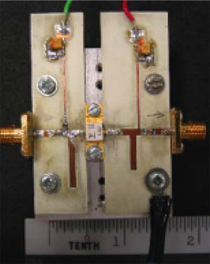
The goal of the Fujitsu FLL357ME power device is to achieve 11 dB of gain and an output power of 35.5 dBm with a PAE of at least 46 percent. The performance of the device is first verified under small-signal conditions, which was tested without any matching network, as shown in Figure 1. The substrate used was Roger’s RO4350, having a thickness of 0.762 mm and relative permittivity of εr = 3.48. All printed circuit boards (PCB) were milled using the Quick Circuit System from T-Tech Inc. The DC bias circuit is designed based on the bias network proposed by Y. Wei, et al.2 to minimize the physical dimension of the PCB. The equivalent circuits of the lumped components were used in the simulation. The PCBs are mounted on an aluminium plate for RF ground and heat-sinking.
 | ||
| Fig. 1 A Fujitsu power device tested with 50 Ω lines at the input and output. | ||
The S-parameters provided by the manufacturer and that measured at 10 V, 720 mA are shown in Figure 2 for comparison. On the right Y-axis, the measured Rollette stability factor K is greater than 1, implying that the device is unconditionally stable from 1 to 3 GHz.
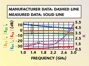 | ||
| Fig. 2 Comparison of S-parameters and K value measured and provided by the manufacturer. | ||
Based on the small-signal S-parameters provided by the manufacturer (with a test data of P1dB = 34.98 dBm), the power amplifier (PA) is designed by applying the conjugate impedance matching technique3 for maximum gain at 2.212 GHz. The matching circuit was simulated and optimized using Agilent’s ADS 2003. The layout of the fabricated amplifier is shown in Figure 3.
 | ||
| Fig. 3 Layout of the power amplifier matched for maximum small-signal gain. | ||
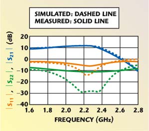
The simulated and measured small-signal S-parameters are shown in Figure 4. The gain measured at 2.212 GHz is improved from 5.9 to 12.8 dB. However, the P1dB of the amplifier measured at 2.212 GHz is approximately 33.4 dBm, as shown in Figure 5.
 | ||
| Fig. 4 Simulated and measured S-parameters of the power amplifier matched for maximum small-signal gain. | ||
 | ||
| Fig. 5 Power characteristics of the power amplifier matched for maximum small-signal gain. | ||
Passive Load Pull
Though the gain of the PA is achieved, the P1dB of the PA is 33.38 dBm due to the fact that the matching is done for maximum transducer gain, not necessarily the required load impedance for optimum output power from the PA. To locate the actual load impedance needed for optimum power output, a Maury Microwave slide screw tuner (model 2640D1) was connected at the output of the amplifier before the power meter. The complete set up is shown in Figure 6. A driver amplifier was used to ensure that the test input power to the PA is consistent at 23 dBm at 2.212 GHz. The design procedure is as follows:
Step 1: Driving the PA with the appropriate test power and fixed DC biases, the tuning stubs and slider of the tuner were adjusted until maximum power was observed on the power meter.
Step 2: The phase delay of the SMA connector was found using a vector network analyzer at the design frequency. The reference plane at the VNA was shifted to de-embed the effect of the SMA connectors and then the output-matching circuit of the PA together with the tuner was connected to the VNA, as shown in Figure 7.
Step 3: The load impedance displayed on the Smith chart at the design frequency was recorded. Based on the load impedance measured, the output-matching network was optimized for this load impedance using an EDA software tool.
Step 4: The output-matching network is integrated on the PA device.
 | ||
| Fig. 6 Set up for passive load pull. | ||
 | ||
| Fig. 7 Set up to measure the required output load impedance of the power device. | ||
Implementation and Measurement
Step 1: The Fujitsu power device is biased at Vds = 10 V, 0.54 A, Vgs = –1.3 V (manufacturer’s recommendation).
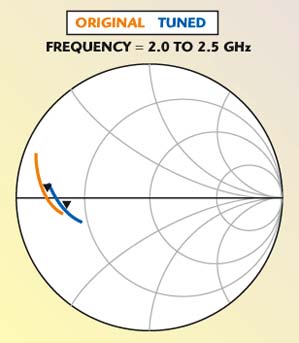
Step 2: The phase delay due to a SMA connector is approximately 32.23° at 2.212 GHz. With the effect of the SMA connector de-embedded, the measured load impedance of the PA device is found to be approximately 6.51 Ω at 2.212 GHz, denoted in blue in Figure 8.
Step 3: Using narrowband transmission line matching techniques, the output-matching network was optimized using ADS 2003 to match to the required load impedance measured at 2.212 GHz. The optimized output-matching network is designed and simulated via small-signal S-parameter analysis in ADS. It is matched to the measured load impedance at 2.212 GHz, which is 6.51 Ω for optimum output power from the PA device used in step 1. It can be seen that the initial design was matched to 20.94+j3.37 Ω for maximum gain. This explains why the P1dB measured for the PA optimized for small signals is below specification at 33.38 dBm.
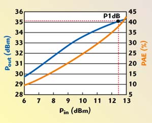
Step 4: The output-matching network for optimum output power is incorporated into the final PA design. The final PA circuit is shown in Figure 9. The measured P1dB is 35.35 dBm, close to the manufacturer’s specification of 34.98 dBm.
 | ||
| Fig. 8 Measured and simulated load impedances for optimum power output and maximum gain. | ||
 | ||
| Fig. 9 Final power amplifier circuit for optimized output power. | ||
On-board Tuning of the PA Circuit
Based on the same optimized output-matching network, another PA device from the same manufacturer (with test data of P1dB = 35.37 dBm) is used for the second PA circuit. The measured output power of the PA is now +34.6 dBm. By repeating steps 1 to 3, it has been found that for the second PA device, the optimum load impedance is now 10.6 Ω instead of the 6.51 Ω for the first PA device.
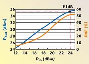
Since the load impedance is higher, the length of the output open circuit stub must be shortened. Connecting the output PCB and with a 50 Ω termination, it can be seen in Figure 10 that the load impedance is 6.32 Ω initially for the second PA circuit. The length of the stub was trimmed by approximately 3 mm and the load impedance measured on the Smith chart is now 11.48 –j4.6 Ω. If a lower impedance is required, the open circuit stub can be extended by soldering a small piece of copper tape from the open stub to the rectangular patches next to the stub. By trimming the output open circuit stub of the second PA as described earlier, the measured P1dB is now 35.42 dBm with a PAE of 52 percent, as shown in Figure 11.
 | ||
| Fig. 10 Load impedance of the second PA measured before and after tuning. | ||
 | ||
| Fig. 11 Performance of the second optimized power amplifier measured at 2.212 GHz. | ||
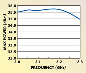
The maximum output power of the optimized PA, biased at a Vgs of –1 V and Vds of 10 V, is shown in Figure 12. The maximum output power is greater than 35 dBm from 2.0 to 2.3 GHz.
 | ||
| Fig. 12 Maximum output power vs. frequency for the optimized power amplifier. | ||
Table 1 summarizes the measured performance and the manufacturer’s test data for the two PAs. It is noted here that their optimum load impedances for power performance are different.
 | ||
Performance of the Integrated PA with a Driver Amplifier and a 20 dB Coupler
The design presented in this section demonstrates the flexibility of the approach to locate the actual load impedance when the PA is integrated with other microwave circuits. In this design, a driver amplifier (WJ Communications Inc., AH102) is connected to the input of the PA and a 20 dB coupler is connected to the output, as shown in Figure 13. The driver amplifier was built and tested separately. The measured P1dB of the driver amplifier is approximately +25 dBm with a gain of 11.8 dB at 2.212 GHz. The insertion loss of the 20 dB coupler is approximately 0.3 dB.
 | ||
| Fig. 13 The integrated power amplifier, driver amplifier and 20 dB coupler. | ||
As expected, the measured output power is below the targeted goal due to variation of the optimum load impedance of the power device. The load impedance was optimized by repeating the procedure that has already been explained in a previous section and the on-board tuning of the integrated PA circuit was performed. At 2.212 GHz, the output power measured with a power meter at the output of the integrated circuit is shown in Figure 14.
 | ||
| Fig. 14 Performance of the integrated power amplifier circuit measured at 2.212 GHz. | ||
The output power of the integrated PA, biased at Vgs = –1 V and Vds = 10 V, is shown in Figure 15. The output power of the integrated PA decreases as frequency increases due to the fact that the gain of the driver amplifier decreases with increasing frequency.
 | ||
| Fig. 15 Output power vs. frequency for the integrated power amplifier. | ||
Conclusion
The PA design becomes flexible and easy with this approach, especially when the device is cascaded with other microwave circuits. The approach described here is easy to implement with minimal effort even without a complete load-pull system. The characterization of a power device is impossible using this method; however, it demonstrates how a PA can be designed and implemented using a VNA and a slide screw tuner.
References
- Maury Microwave Corp., Application Note MT956D, “Measurement of Large-signal Device Input Impedance During Load Pull,” 6 Nov 1998.
- Y.Y. Wei, P. Gale and E. Korolkiewicz, “Effects of Grounding and Bias Circuit on the Performance of High Frequency Linear Amplifiers,” Microwave Journal, Vol. 46, No. 2, February 2003, pp. 98–106.
- D.M. Pozar, Microwave Engineering, Second Edition, John Wiley & Sons Inc., Somerset, NJ, 1998, pp. 618–622.
Yeap Yean Wei received his B.Eng. degree in communication and electronics engineering with first class honors from Northumbria University, UK, in 2002. He has been working as a project officer in the Satellite Engineering Center, NTU, since December 2002. His current job responsibilities include design, prototyping and integration of an X-band, high bit rate, transmitter and S-band telemetry and telecommand transceiver.
Chua Lye Heng received his B.Eng. (honors) and M.Eng. degrees in microwaves from the National University of Singapore in 1987 and 1995, respectively, and his PhD degree in electronic systems engineering from the University of Essex, Colchester, UK, in 2003. His research interests include filters, microwave and millimeter-wave planar structure analysis, HMIC and MMIC design.