
Thermal management in microwave printed-circuit boards (PCB) is more important than ever, with the growing demand for higher levels of circuit integration and PCB power densities. Understanding proper thermal management of a microwave PCB requires some basic theory regarding heat flow in a PCB, as well as the thermal properties of the materials used in PCBs. To illustrate PCB thermal management in practical terms, an experiment will be detailed to show the heat flow in a PCB at various power levels and using materials with a variety of different thermal properties. As an example, a simple microstrip circuit will help to illustrate heat flow through a PCB, including the effects of plated-through-hole (PTH) via holes (vias) used for signal-ground connections in isolated areas of the PCB.
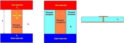
Figure 1 Basic heat flow models.
A basic thermal model can be described by hot and cold areas or reservoirs connected by a thermally conductive material, such as copper (see Figure 1). Copper has a thermal conductivity (TC) of approximately 400 W/m/K, which is considered to be very good. For a model that more closely resembles the thermal flow in a microstrip PCB with PTH via hole, the basic model is modified by having thermal insulators now surrounding the thermal conductor, with the PCB substrate serving as the thermal insulator (Figure 1b); a PCB substrate generally has a TC of approximately 0.25 W/m/K. In creating a model for a microstrip PCB (Figure 1c), the top copper layer is assumed to be the signal layer (or the hot reservoir) while the bottom copper layer is assumed to be the ground plane (or the cold reservoir).
In this basic thermal model, the relationship for the transfer of heat between the hot and cold reservoirs is:

where H is the heat flow, k is the thermal conductivity, A is the area at the reservoir-thermal conductor interface, ΔT is the heat difference and L is the length of the thermal conductor joining the reservoirs. In this model, it is assumed that the temperature in the thermal conductor has reached equilibrium. The simple model and the equations indicate that less heat transfer will occur between reservoirs for a thermal conductor with low thermal conductivity. The distance between the reservoirs will also impact the amount of heat transferred, while a thinner thermal conductor will increase heat flow.
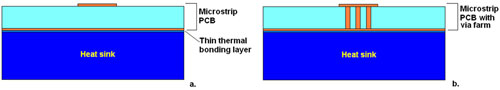
Figure 2 Cross-sectional views of a microstrip PCB: (a) without via farm and (b) with via farm.
Fitting this simple model to a microstrip PCB, the PCB's signal layer is assumed as the hot reservoir and the PCB's ground plane is the cold reservoir (see Figure 2). It is also assumed that the ground plane is thermally attached to an efficient heat sink to maintain a constant temperature, which is significantly lower than the signal plane.
The areas of a microstrip PCB may be with or without PTH via holes. A model corresponding to a microstrip PCB in an area with no PTH via holes is shown in Figure 2a, while a model representing a microstrip PCB in a grounded area, where numerous PTH via holes are used to join two copper layers, is shown in Figure 2b. The model of Figure 2(b) is common for microstrip PCBs on which an active device, such as a power transistor, is mounted and is generating heat. The numerous PTH holes under the heat generating device is called a via farm.
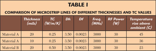
When several materials with different thicknesses and TC values are compared, as in Table 1, and other key parameters are kept the same, such as input test power and frequency, the impact on the thermal rises of those different materials is easily seen. For example, the three materials in Table 1 are treated with similar values of relative dielectric constant (Dk) and dissipation factor (Df), and the same frequency (3000 MHz) and power level (30 W). There are no grounding via holes in any of the materials, but the temperature rise above ambient is different for all three materials, depending upon material thickness and TC value. The highest temperature rise above ambient occurs for the thickest PCB material with the lowest TC value. In this model, which is known to be very conservative but valid for the sake of this simple comparison, there is no grounding via hole.

As Table 1 shows, PCB materials with a lower value of TC suffer a higher temperature rise above ambient for a given amount of applied power, while higher values of TC result in lower temperature rises above ambient. Some of the TC values for materials commonly used in high frequency PCBs are shown in Table 2. Unfortunately, most of the PCB materials used in the microwave industry exhibit relatively low TC values.
In terms of thermal conductivity, laminates, such as RO4350B™ and RT/duroid® 6035HTC from Rogers Corp., offer high values, compared to FR-4 substrates often used in high frequency circuits. Still, the TC of conductive copper metal is about 400 W/m/K, some orders of magnitude higher than the TC values for any of the substrates in Table 2. This shows that copper PTH vias can have a major impact on the heat flow within a microwave PCB.

Figure 3 Comparison of heat rise above ambient with substrates having different TC values.
To understand the effects of TC for different PCB materials, a thermal imaging study was performed using microstrip constructions and different substrate materials with significantly different TC values. Heat flow effects for these materials were also studied with and without via farms. DC heating was used to eliminate several microwave thermal variables and focus on the effects of TC on different PCB materials. All substrates in the study were 20 mils thick with a 100 Ω termination resistor and the same copper features, although different substrate materials were used. Once DC power was applied, each circuit and termination resistor was allowed to reach thermal equilibrium. Figure 3 shows the difference in heating above ambient temperature (25°C) for circuits without a via hole farm, using different materials. As seen in Figure 3, and referenced in Table 2, materials with the highest TC values exhibit the lowest temperature rises. When these curves are compared to circuits using via farms, which can channel some of the heat, the heat rise is less for each circuit, although the general trends are the same.

Figure 4 Cross-sectional views of microstrips: (a) without via farm, (b) with via farm and (c)with a via fence.
Figure 4 shows cross-section views of the microstrip example (a) without via holes, (b) with a via farm, and (c) with a via fence. The microstrip without via holes is typically of an RF signal, where the active signal trace cannot be connected to the ground plane. In this case, the TC property of the material is critical for minimizing the heat rise. Of course, a thinner substrate will also shorten the heat flow path and reduce the heat rise of the circuit.
For microstrip circuits with active devices that generate heat, the configuration in Figure 4b, with via holes, is commonly used to improve thermal dissipation. An active device may require ground connections anyway, so the use of copper PTH via holes as thermal connections from the active device to ground can greatly aid the thermal management of the PCB.
The microstrip PCB configuration shown in Figure 4c is somewhat more uncommon than the other circuits. According to the area of the cross-sectional view, the circuit configuration of Figure 4c is more like a grounded coplanar waveguide than microstrip, with the benefit of allowing active circuit traces that cannot be grounded by means of via hole connections to dissipate heat by means of PTH via holes through x-y plane thermal conduction. In such a case, the substrate material's TC value is critical for optimum heat dispersion. In this circuit configuration, the spacing on the signal plane between the active trace and the coplanar ground with the via hole fence should be small compared to the substrate thickness. The spacing can be in the range of 125 μm (5 mils). By minimizing the heat flow path, the transfer of heat from an RF signal trace to the ground plane is made more efficient. In this configuration, some electrical concerns must be addressed regarding the close proximity of the coplanar ground to the signal trace.
One part of proper thermal management in microwave PCBs involves understanding the relationship between circuit losses, applied power and heating effects. High frequency circuit heating is essentially associated with losses in the circuit. And in microstrip circuits, such as the example, there are several types of losses, including conductor losses, dielectric losses and radiation losses. Conductor losses are related to the circuit design as well as the choice of substrate. Most substrates are available with different types of copper cladding and the choice of copper can impact the loss performance. For example, copper conductors with rough surfaces will suffer higher losses than copper conductors with smooth surfaces. The quality of the copper-substrate interface can also impact the loss performance of a microstrip PCB.
Another material parameter that can affect loss is a PCB material's Df. A lower value for Df results in less dielectric loss and less heat generated in the PCB. In addition, a PCB with low Dk will also yield less loss and less generated heat than materials with higher Dk values. This is assuming that a controlled-impedance circuit design is necessary and a material with a lower Dk allows the use of wide conductors. Wider conductors yield lower conductor losses than narrower conductors.
In brief, a short list of ideal material properties for improved thermal management includes high TC, low Df, smooth copper surface, thin laminate and low Dk. Of course, in practical designs, there are always tradeoffs involved. An example can help to demonstrate this. This example employs a 20 mil microstrip transmission line on a substrate with Dk of 3.5 and handling 30 W RF power at 3 GHz. The circuit is required to achieve good low loss performance. It is based on a ceramic-filled PTFE substrate with Df of approximately 0.0023. Because of the high cost of PTFE material and its associated fabrication processing, a lower cost alternative substrate was considered for the example, a hydrocarbon laminate with Df of 0.0037.
Using a simple model to compare the substrates, the predicted temperature rise above ambient temperature is approximately 45°C for the PTFE substrate and approximately 21°C for the hydrocarbon laminate. Although the PTFE substrate has a lower Df than the hydrocarbon laminate, the latter has a lower heat rise due to its TC value of 0.62 W/m/K compared to only 0.25 W/m/K for the PTFE laminate.
The maximum operating temperature (MOT) of a microwave PCB is an important parameter to consider as part of thermal management planning for a circuit design. Determined by a certification process from Underwriters Laboratory (UL), the MOT cannot be exceeded for any length of time to ensure the integrity of the PCB. Short-term elevated temperatures associated with soldering and assembly are not related to the MOT. Rather, it is long-term issues, at higher temperatures, that are a concern for achieving thermal management with a microwave PCB. In fact, MOT can be used in a simple circuit model to illustrate some differences in materials when considering a 20 mil microstrip transmission line.
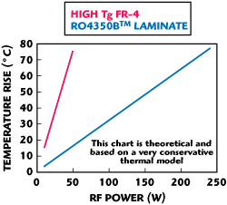
Figure 5 Example of a 2-mil microstrip line using two different substrate materials.
The MOT in this example circuit is assumed to be +105°C, and the ambient (room) temperature is +25°C. The goal in this example is to avoid a temperature rise of more than 80°C, in order not to violate the MOT for this material. As Figure 5 shows, the choice of PCB material can greatly impact the amount of power that can be carried by a microwave circuit, with materials having higher TC values and lower Df. The example is based on a frequency of 800 MHz; at higher frequencies, more heating will occur for the same RF power level. While the conductor copper roughness mentioned earlier may have minimal effects at lower frequencies, it can impact losses more at higher frequencies, translating into additional heat generated in a PCB with copper conductors having a rough copper surface.
In summary, it is possible to envision heat flow through a high frequency PCB by means of a simple model. Using such a simple model helps illustrate the benefits of circuit materials with high thermal conductivity and can help when developing strategies for effective PCB thermal management. Via farms can be an effective method of improving heat flow through a PCB, although it may not always be possible to employ this technique with active RF signal traces. In general, attention to selecting circuit material with favorable attributes, such as improved TC, low dissipation factor, smooth copper conductor surface and low dielectric constant, cannot only help in the design of a high performance PCB, but also lead to improved thermal management.