
Enhancement-mode PHEMTs significantly extend the usefulness of GaAs RFICs for general-purpose RF component designs. To demonstrate the technology’s benefits, this article demonstrates a 2 to 3 GHz GaAs PHEMT RF pulse modulator operating off a single, positive supply voltage, switched by a TTL-level logic signal. Active gate bias networks, designed using feedback techniques, provide exceptional stability of performance over a wide range of supply voltages and harden the RFIC against severe levels of radiation. Although greater levels of integration are easily achieved using RFICs, this design highlights the flexibility and robustness of the RFIC approach for “drop-in” component designs.
The modernization of legacy hardware is an important activity for RF/microwave designers in the aerospace industry. The task of upgrading a legacy system can include replacing a single RF component, a chain of components, or an entire RF transmitter/receiver. Signal processing, digital control and available power supplies may or may not be “off-limits” for the redesign. Depending on tradeoffs and limitations involved, the design approach generally can take one of two different courses: Commercial-off-the-shelf (COTS)-based design or custom radio frequency IC (RFIC) design. Combinations of the two approaches are also possible.
COTS devices range from RF discretes to multifunction ICs. They typically come in plastic encapsulated packages (PEMS) and ceramic packages with pedigrees ranging from commercial grade though military/space qualified. The COTS approach can be extremely cost effective if design requirements conform to the functionality of commercially available products. But if customization is unavoidable, the total number of required components can rapidly proliferate with associated penalties in size, weight, power, qualification time, reliability and cost.
An alternative approach is to replace legacy components/systems with application-specific RFICs. There are advantages to this. RFIC designs can easily meet custom requirements; for example, a receiver output signal specifically conditioned for an existing signal processor. Greater margins of operation can be achieved using foundry-validated device models and controlled on-chip parasitics; for example, broader bandwidth, temperature compensation, or reduced sensitivity to supply variation. Such performance advantages can even allow RFICs to be “over-designed” for a particular application in order to permit reuse on multiple projects, thus reducing long-term development costs. Proprietary RFIC chipsets can also protect against component obsolescence, which currently costs the US Department of Defense $10 B per year.1
Perhaps the most important advantage to RFIC-based design are the manufacturing improvements: Minimized part count, enhanced reliability, reduced qualification time, less vendors and a production process compatible with industry best practices.
Today’s RFICs come in various flavors of gallium arsenide (GaAs) and silicon. Each technology has its benefits. In the case of silicon, the advantages are p-type devices, analog/digital integration, lower power consumption, smaller circuit size and improved cost/yield in high volume applications. The benefits of GaAs, on the other hand, are higher breakdown voltage, improved output power and power handling, higher-Q on-chip passives, inherent radiation hardness, longer sunsets for old processes, far less expensive software design flows, and—depending on the type of process chosen—surprisingly low cost for small and medium volumes.
Recently, the usefulness of GaAs RFICs for insertion in legacy systems has increased due to advances in the RF performance and producibility of enhancement-mode PHEMTs (E-PHEMT). Unlike conventional depletion-mode GaAs devices, E-PHEMTs have positive threshold voltages that allow much greater flexibility in biasing and control—a feature particularly relevant for designs targeting the replacement of existing components.
This article demonstrates the advantages of E-PHEMT RFICs for a basic “drop-in” component design—an RF pulse modulator. The pulse modulator is designed as a gate-switched two-stage amplifier running off a single, positive power supply. A TTL-level logic signal provides the control. Measured results show greater than 26 dB gain in the on-state and greater than 79 dB on/off isolation over the entire 2 to 3 GHz band. The detected rise/fall times are less than 13 nsec. Active bias circuits and feedback allow the circuit to maintain good performance and output power over a wide range of voltages and under severe radiation conditions. These results are expected to offer many practical advantages for RF component design in a variety of aerospace applications.
Design

Figure 1 Transfer curve of a 0.5 µm E-PHEMT biased at Vds = 7.2 V.
The design shown in this article uses TriQuint Semiconductor’s TQPED process (0.5 µm enhancement and depletion mode PHEMTs). Competing technologies are also available from other vendors. The ft and fmax of the E-PHEMT devices are 33 and 100 GHz, respectively; the minimum guaranteed breakdown voltage is 15 V. Figure 1 illustrates the transfer curve of a TQPED E-PHEMT for a Vds of 7.2 V. The threshold voltage is +0.35 V; 0 V on the gate can easily turn off the device. An Imax of 320 mA/mm occurs at approximately Vgs = 1 V.

Figure 2 GaAs FET active bias circuit for a common-source connected device Q1.
The E-PHEMT’s positive threshold voltage makes it possible to design a single-supply active bias with reasonable immunity to thermal drift or supply voltage variation. Figure 2 illustrates a network for biasing a common-source connected GaAs FET; similar topologies are described in the literature.2-4 The objective is to control the bias point for the RF transistor Q1. Q2 acts as a current mirror. R4 sets the value of the current in Q2. Depending on the options available, this resistor should be selected to have a low variation with temperature at the expense of resistor size. Transistor Q3 provides an additional, strong feedback; the diodes and Q4 are used simply to provide a known voltage drop. Note that, unlike MOS devices, there is a gate current that varies with temperature. Because of this, the RF stability resistor R1 should be kept to as low a value as practical, in order to reduce the bias point’s sensitivity to temperature drift and process variations that would affect the gate current (that is, variations in threshold voltage). Furthermore, it is important to scale R1 and R2 according to the gate currents in Q1 and Q2 in order to have identical gate-source voltages for both devices. The appropriate scaling relationships are
EQUATION 1
where WQ1 and WQ2 are the total channel widths of transistors Q1 and Q2, respectively. ID,Q1 and ID,Q2 are the drain currents, and IG,Q1 and IG,Q2 are the gate currents.

Figure 3 Complete schematic of the GaAs E-PHEMT pulse modulator.
Figure 3 illustrates the schematic of the complete pulse modulator. The design is a two-stage amplifier with gate switching and independent active biasing for each stage. The nominal drain voltage is 7.2 V and the operating bandwidth is 2 to 3 GHz. The active bias networks are optimized to provide a stable class-A operating point for each common-source amplifier stages over a ±15 percent variation in supply voltage and a -55° to +80°C variation in temperature. Both common-source amplifier stages are 8 × 50 µm devices. The first stage is reactively matched at the input. The second stage uses a negative feedback in order to make the output power level/match insensitive to process variations or model errors. The shunt switch FETs at the gates of both common-source stages can switch the amplifier on and off. Referring to the transfer curve, when the control signal is 0 V, the shunt switches are open and the amplifier is on. For a +3 V control signal, the shunt switches are closed and the amplifier is off. Note that the resistive tees at the gates of both switch FETs serve multiple purposes: (i) to divide down the +3 V control voltage so that the switch FETs cannot exceed Imax; (ii) to provide broadband attenuation to prevent loop oscillations between the first and second amplifier stages; and (iii) to RC filter the control signal. The shunt capacitance in parallel with each resistive tee is 20 pF, which is a tradeoff between switching speed and the level of RC filtering.

Figure 4 Chip layout in Agilent ADS.

Figure 5 The fabricated RFIC integrated into an existing multilayer LTCC module.
Figure 4 shows the chip layout as it appears in Agilent ADS.5 The chip size is constrained to 1.75 × 3.5 mm by the size of other chips on a multi-project run. Because this chip area is far greater than required for the design, over 325 pF of on-chip bypassing is added to the layout. The RF input and output pads are asymmetric for compatibility with an existing module design. Note that the first and second stage VDD and control pads are separate on the chip for testing purposes, but combined at the module level. Also, the “L”-shaped pads placed at the upper left and lower right corners serve as auto-recognition fiducials for robotically-controlled wire bonding in the production environment. Figure 5 shows the fabricated RFIC integrated into a previously existing multilayer LTCC module. As mentioned, the module had already been manufactured for an earlier pulse modulator design.
Performance

Figure 6 Small-signal response of the pulse modulator in the on- and off-states.
The RFIC is tested at the die level on a manual wafer probe station. All the instrument grounds are tied directly to the RFIC backside ground on the wafer prober. The force/sense lines, connecting the power supply outputs to the DC probes, reference all measured voltages and currents to the DC probes. The power meter and S-parameter measurements are referenced to the RF probe tips, using off-chip SOLT calibration standards. Figure 6 shows the small-signal frequency response of the pulse modulator for the on- and off-states. The results for five randomly selected RFICs are shown. Across the 2 to 3 GHz band, the maximum return losses are better than 10 dB. The gain decreases from 28 dB at 2 GHz to 26 dB at 3 GHz; the minimum on/off isolation decreases from 85 dB at 2 GHz to 79 dB at 3 GHz.
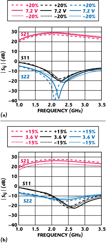
Figure 7 Variations in the on-state small-signal response for 7.2 V ± 20% (a) and 3.6 V ± 15% (b).

Figure 8 Variations in the on-state output power for 7.2 V ± 20% (a) and 3.5 V ± 15% (b).
As shown in Figure 7, when the supply voltage drifts by ±20 percent from the nominal 7.2 V, the amplifier is still matched across the 2 to 3 GHz band, and the gain remains above 25 dB. In fact, the figure also shows that the design maintains good performance over the same band, even when using a 3.6 V supply varying ±15 percent. For both cases, the off-state S21 remains unchanged from its value at the nominal power supply voltage. The relative insensitivity of the design to supply variations is further illustrated by the power measurements shown in Figure 8. At 7.2 V, the P1dB is 21 dBm with a current draw of 59 mA. At 3.6 V, the P1dB is 17 dBm with a current draw of 18 mA. This stability of performance across a wide range of supply voltages testifies to the robustness of the feedback designed into the active bias network and to the effectiveness of the negative feedback used for the output match.

Figure 9 Output time domain waveforms.
For dynamic testing, the pulse modulator is switched on and off with a low-level TTL signal (0 V, +3 V) generated by an Agilent 81111A signal generator. The envelope of the detected RF waveform is shown in Figure 9 under small-signal drive conditions as well as at P1dB. For a CW input frequency of 2.5 GHz, the slowest rise/fall times observed are for the small-signal case: 12.6 nsec rise (10 to 90 percent) and 7.8 nsec fall (90 to 10 percent).
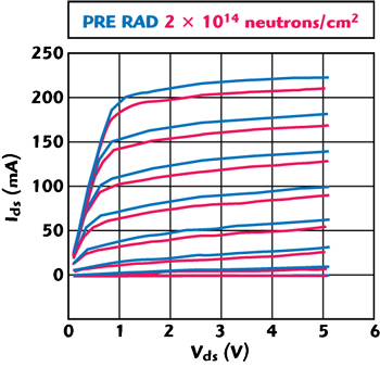
Figure 10 Characteristic I-V curves for 6 × 50 µm device before and after exposure to a 2 × 10¹⁴ neutrons/cm2 radiation.

Figure 11 Small-signal gain of the pulse modulator RFIC before and after radiation exposure.
The active bias networks that make this design robust against wide variations in supply voltage also serve to harden the design against severe radiation exposure. GaAs is electrically insulating and therefore inherently hard against several forms of radiation. In Figures 10 and 11, an individual 6 × 50 µm PHEMT and the overall pulse modulator RFIC are subjected to a fluence of 2 × 10¹⁴ neutrons/cm2.6 The individual device shows some degradation after exposure to this high level of neutron radiation, but the effect on the gain of the on-state pulse modulator is negligible for all practical purposes.
Conclusion
The RF pulse modulator described in this article demonstrates some of the benefits and techniques possible using E-PHEMTs technology: Single-supply operation, TTL-level logic control and active bias networks. The RFIC shows good gain and output power over the entire 2 to 3 GHz bandwidth. Worst-case switching times are less than 13 nsec. The performance remains stable over a wide range of supply voltages and under severe radiation conditions. Although much greater levels of integration are possible, these results illustrate the flexibility and robustness of GaAs RFICs for the replacement of existing RF component/subsystem hardware.
Acknowledgments
The authors wish to thank C. Sandoval and M. Armendariz for including this device in radiation testing. They also thank J. Dimsdle and S. Sedlock of Honeywell Federal Manufacturing and Technologies as well as P. Litzenberg and K. Mays of TriQuint Semiconductor for helpful technical discussions.
Sandia National Laboratories is a multiprogram laboratory operated by Sandia Corp., a Lockheed Martin company, for the United States Department of Energy’s National Nuclear Security Administration under contract DE-AC04-94AL85000.
References
1. P. Sandborn, “Trapped on Technology’s Edge,” IEEE Spectrum, Vol. 45, No. 4, April 2008, pp. 42-58.
2. D. Criss, “TriQuint Semiconductor Foundry Customer Course Notes,” January 2005.
3. P.R. Gray, P.J. Hurst, S.H. Lewis and R.G. Meyer, Analysis and Design of Analog Integrated Circuits, 4th Edition, John Wiley & Sons Inc., New York, NY, 2001.
4. C. Tomazou, F.J. Lidgey and D.G. Haigh, Analogue IC Design: The Current-mode Approach, Peregrinus, London, UK, 1990.
5. “Advanced Design System 2005A,” Agilent Technologies Inc., Palo Alto, CA.
6. M.G. Armendariz, C.E. Sandoval and M.A. Montano, “Triquint RFIC Radiation Characterization,” US Dept. of Energy Report, SAND2007-7920.
Christopher T. Rodenbeck received his BS, MS and PhD degrees in Electrical Engineering from Texas A&M University, College Station, TX, in 1999, 2001 and 2004, respectively. His graduate studies were supported, in part, by fellowships from NASA, the State of Texas “to advance the state of the art in telecommunications,” Texas A&M and TxTEC. He is currently a senior member of the technical staff at Sandia National Laboratories, Albuquerque, NM, where he works on the design of antennas, radio frequency integrated circuits and multichip modules.
Richard T. Knudson is a distinguished member of the technical staff at Sandia National Laboratories, with more than 30 years of experience in RF/microwave circuit design for advanced radar applications.