
In today's global wireless industry, demands for semiconductor performance are becoming increasingly more challenging. Higher power and higher operating frequencies are two themes that permeate throughout this market space. Applications such as Magnetic Resonance Imaging (MRI) and UHF/VHF Tactical Radios require extremely high power handling PIN diodes at lower frequencies. Alternatively, broadband and high frequency applications such as Test Instrumentation, RADAR and Sensors require PIN diodes to push frequency ranges beyond 70 GHz.
PIN diodes typically come in several semiconductor flavors-Silicon, GaAs and AlGaAs. Not only does the semiconductor process play a significant role in the performance of PINs, but also the packaging medium. Many suppliers have subsequently developed unique process and packaging technologies designed to address the various frequency, power and mounting needs of customers. Three PIN diode products that have pioneered the diode industry are Silicon Metal Electrode Leadless Face (MELF) packaged PINs for high power applications, packageless PINs for broadband surface-mount applications, and flip chip AlGaAs PINs for ultra-high frequency applications. In this paper, the processes and packages of these devices will be explored, compared and contrasted.
MELF PIN Diodes

Figure 1 MELF package construction.
MELF package PIN diodes were designed with the intention of operating in high power, low frequency environments. The rugged MELF design hermetically encloses the PIN diode in ceramic, as shown in Figure 1. The diode is sandwiched between two Molybdenum plugs from the top and bottom. With a thermal conductivity at 208C of 142 W/mK, these Moly plugs provide an optimal thermal contact with the diode die to facilitate heat conduction. A solder preform is then added on the external side of the plug. The combination of this RoHS solder preform and the metallized ceramic on the top and bottom of the package allows for these devices to be surface mounted using Sn63/Pb37 solder or some other RoHS compliant solders. The tin plated, rectangular construction was done intentionally to enhance solderability and aid in high volume, pick and place environments.

Figure 2 Silicon PIN diode construction.
The construction of the MELF PIN is critical to an RF designer due to the efficient heat dissipation and consequent power handling up to 200 W. In addition, PIN diodes with different I-region thicknesses ranging from 30 to 350 micron can be mounted into this package style. Thicker I-regions handle higher RF voltages and provide higher linearity (IIP3) due to the increased breakdown voltage (Vb). In contrast, thinner I-regions will have faster switching/settling speeds as well as lower series resistance (Rs). Figure 2 shows the construction of the PIN diode. These MELF PINs work well down to 300 kHz and up to about 2 GHz before package parasitics impact their RF performance.

Figure 3 MELF package styles.
MELF PIN diodes have two package styles, as shown in Figure 3. The first is the smallest MELF with a parasitic capacitance of 0.16 pF and a parasitic inductance of 0.15 nH per Moly plug. Figure 4 shows the DC and RF performance of a typical MELF PIN with the DC parameters measured by an impedance analyzer on a single diode, and the S-parameter performance measured on a vector network analyzer. The series resistance, capacitance, insertion loss and isolation are shown for a MELF PIN soldered down onto a Rogers 4350 microstrip line in series. Insertion loss and isolation are also shown for a shunt MELF PIN soldered to ground. Combining both series and shunt MELF PINs into a single configuration shows that the isolation improves dramatically without significantly degrading the insertion loss.

Figure 4 DC and RF performance of a MELF PIN diode.
The performance can be optimized for both bandwidth and high frequency performance very easily with additional matching elements. These PINs are typically used as building blocks for more complex circuits such as multi-throw RF switches and attenuators. The low Rs is critical for low insertion loss series switching applications while the low distortion versus forward current is equally as important for attenuator applications.
These diodes are also available in non-magnetic packages for MRI applications, which require high voltage handling below 1 GHz. The existence of magnetic materials in a PIN diode structure distorts the static magnetic fields associated with various coils and will interfere with calibration and accuracy. Consequently, non-magnetic MELFs have the ability to optimally receive low power return signals from the human body.
HMIC Surmount PIN Diodes
M/A-COM Technology Solutions has developed a Heterolithic Microwave Integrated Circuit (HMIC) process. It is a silicon and glass-based process that uses silicon pedestals embedded in a low loss, low dispersion glass. Selective backside metallization is utilized with via connectivity to the topside RF traces and air-bridges to produce a surface-mount device. The topside of the die is fully encapsulated with silicon nitride, and has an additional polymer layer to help protect against damage during handling and assembly. This surface mountable solution effectively created is called "surmount" throughout this article. A cross-section of the HMIC process as applied to both series and shunt configured PIN diodes is shown in Figure 5.

Figure 5 HMIC process cross-section.
The shunt diode is realized with the anode, cathode and "I" region contained within a silicon pedestal. The cathode of the PIN diode serves as an electrical contact to the ground plane, and since silicon has a thermal conductivity approximately one third that of gold, acts as a low thermal resistance heat spreader. In addition, HMIC provides a simultaneous cathode contact on the top surface of the via enabling more complex switch configurations to be realized. Silicon vias to achieve vertical connections (front to back) are a natural consequence of the HMIC fabrication process. The top surface of these vias typically serves as the "active" layer for the formation of the required diode-based active devices and as interconnection paths for the requisite passive elements. The various circuit elements, either active or passive, are then laterally linked using standard photolithography and metallization techniques.
The shunt diode has the highest power handling so it has a very high thermal conductivity from the surface to ground since its cathode is directly connected to the backside. A series diode, by contrast, is always the weak thermal link in the design since it has the lowest thermal conductivity. A thermally conductive but electrically insulating epoxy isolates the cathode of the diode from the backside of the entire structure. The formation of the series diode is initially identical in formation to the shunt diode. A cavity is created in the silicon cathode using a selective etch that is then packed with a low dielectric constant, high field strength, silica filled epoxy. This epoxy works very well as a DC and RF isolation medium. The limitation with the surmount diode lies with the silica filled epoxy used to isolate the diode when in series from the RF ground plane. The silica filled material is essentially a thermal open and the only heat sinking that is occurring in the series diode is a result of heat flow along the metallization structures to the nearest silicon via. Using 175°C as the maximum reliable operating junction temperature of the switch, which always occurs at the series diode, the diode insertion loss and thermal resistance become the limiting factors to incident power levels.
Combining glass and silicon enables the high frequency and high power handling properties of the two materials to be optimized while allowing true surface-mount device structures to be produced using standard semiconductor processing equipment and techniques. Glass has a low dielectric constant and a low, high frequency loss tangent, while silicon has high thermal conductivity and low electrical resistance. In addition, both materials have a nearly identical thermal coefficient of expansion.
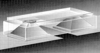
Figure 6 Discrete surmount PIN diode.
When using this process to design discrete surmount PIN diodes, as shown in Figure 6, the shunt construction shown in Figure 5 is used. The anode connection at the top of the pyramid pedestal on the left is connected to an air-bridge. This air-bridge extends over to a via on the right. This via creates an RF connection from the anode through the air-bridge down the via to the backside of the device. The cathode of the diode is also connected to the backside of the device, yielding a direct cathode heatsink and provides for optimal heat transfer. These backside connections also provide for the surface mountable ability. In addition, thermal conductivity and dissipated power are optimized because these diodes are electrically in series, but thermally in shunt. Surmount diodes have I-region widths that range from 10 to 50 microns are available in different sizes. HMIC surmount PINs are useable in MRI applications as they are non-magnetic devices.

Figure 7 S-parameters of a surmount diode.
Surmount PIN diodes can exceed 100 W CW power handling at 2 GHz. The "packageless" surmount construction minimizes parasitic capacitances and inductances to minimal values, resulting in performance from 50 MHz to 26 GHz. Figure 7 demonstrates the broadband small-signal performance of a series mounted surmount diode. Power and bandwidth are two critical attributes and are major differentiators for the HMIC surmount PIN diode option.
Flip Chip AlGaAs PIN Diodes
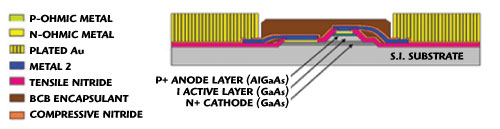
Figure 8 AlGaAs flip chip process.
One chip type that currently transcends multiple semiconductor platforms is flip chip PIN diodes. The AlGaAs diodes combine Aluminum (in the P+ region) and Gallium Arsenide (in the I and N regions), which improves the insertion loss significantly at higher frequency ranges. Due to the reduced recombination rate for electrons and the higher carrier injection rate with an Aluminum-GaAs heterojunction, a greater number of carriers can flow through the I-region, thereby lowering the effective resistivity of the I-region. Fabricated AlGaAs diodes effectively have lower diode "ON" resistance than conventional GaAs devices by as much as 25 percent. Consequently, AlGaAs PIN diodes outperform silicon beam leads and chip devices for a variety of broadband switching applications. Figure 8 shows the vertical construction of the PIN diode and Figure 9 shows several flip chips from the top view.

Figure 9 Flip chips — top view under magnification.

Figure 10 S-parameters of a AlGaAs flip chip.
A flip chip PIN diode connects to a substrate from the top pads of the package. Consequently, the chip has to be flipped and epoxied down to a medium using electrically conductive Ag epoxy. The BCB encapsulant covering the die acts as protection upon the flipping of the diode. This flip chip package construction combined with the AlGaAs process yields a device with capacitance as low as 0.025 pF and operational frequencies beyond 70 GHz. The AlGaAs PIN diode flip chip has good broadband high frequency performance and the fastest switching performance because of its low parasitics and thin I-regions. A common tradeoff with high frequency performance is lower power handling capability, as is the case with flip chips. The PIN diodes are rated up to 23 dBm of CW input power. Figure 10 shows small-signal S-parameter data for a typical AlGaAs flip chip in a series configuration. The device provides significant circuit tuning advantages due to the low total capacitance Ct (< 18 fF), series resistance Rs (4 ohms at 20 mA) and series inductance Ls (0.5 nH). These specifications provide a 0.072 ps RC time constant that affords greater operating bandwidth.
Comparison of Technologies

One major advantage to discrete PIN diodes is that customers are able to easily and quickly customize their diode topology to meet their RF performance needs. Table 1 shows three popular PIN diode switch topologies and each of their strengths and weaknesses. These three switch topologies are the most basic, but there are also designs with multiple cascaded series diodes and multiple shunt diodes on a single arm.

Figure 11 Diode comparison, frequency vs. power.
Figure 11 shows how the three diode processes and packaging technologies compare with each other over frequency and maximum CW input power. The trend in performance is typically the maximum operating frequency and maximum CW incident power are inversely related. The MELF PIN diode can handle up to 200 W of CW incident power, but has the narrowest and lowest frequency band of operation. Alternatively, the flip chip PIN diode has been shown to operate beyond 80 GHz with the broadest bandwidth performance, but with limited power handling of 0.2 W incident power. The optimal compromise between frequency and power was described with the HMIC surmount PIN diodes, which can handle up to 100 W of incident power while still achieving broadband performance up to 26 GHz.
Conclusion
MELF, surmount and AlGaAs flip PIN diodes were described and compared against each other. Each type of PIN diode has clear advantages, depending on the end application. The PIN starting material, I-region thickness and packaging technology play major roles in the diode performance.
 Kevin Harrington holds his MS degree in Electrical Engineering from the University of Massachusetts, Amherst. He brings to M/A-COM Technology Solutions more than 13 years of experience in GaAs RF IC design and five years of product management. He is currently Product Development Manager responsible for HMIC diode & GaAs IC product development across multiple markets.
 Scott Vasquez holds his MS degree in Electrical Engineering from Tufts University. He has been an applications engineer with M/A-COM Technology Solutions for over two years. He is currently a Product Manager responsible for diode-based products.