
Much of today’s R&D in high-frequency electronics is concerned with squeezing more functionality into a smaller package at an affordable price. While large, complex ICs known as System-on-Chip (SoC) are the choice when production volume is high, multi-chip integration often wins for lower volume and speedier time-to-market. The multi-chip approach allows designers to match the optimum IC technology to the required functionality achieving the best performance vs. cost. Better yet, multi-chip design can combine diverse technologies while still delivering a single integrated package or module. But as multi-chip packaging grows in capability, so does the complexity. The prospects for multi-chip design lies in the industry’s ability to adopt the design efficiency and performance that has fueled the IC market. In this report, we will examine the state-of-the-art in miniaturization and advanced high density RF/microwave package design.
Benefits of Multi-Chip and Dense Package Design
With the challenges facing the wireless industry, typified in the latest 3G multimode handset developments, companies such as RFMD, a leading provider of multi-chip devices, anticipate that new processes and enabling technologies such as high-linearity PHEMT, silicon on insulator (SOI), GaAs E/D PHEMT, GaAs HBT and GaAs BiFET will need to be combined with new packaging technologies such as hermetically sealed wafer level packaging (WLP) and integrated RF shielding in order to achieve size reduced solutions. Examples of these more highly integrated cellular product categories include switch filter modules, switch duplexer modules, single placement front-end modules and other high-performance RF components for cellular handsets. Wireless infrastructure, wireless connectivity, broadband/consumer and aerospace & defense applications will also benefit from these enabling technologies as well as another key enabler, gallium nitride (GaN). “Optimum technology matching” is the term coined by RFMD to describe how it aligns various semiconductor technologies to attain the optimum performance for a given RF function.
MCM, SiP and SoP
The terminology describing multi-chip packaging has evolved with the technology itself. Multi-chip modules (MCM) were initially developed for mainframe computers back in the 1980s. These modules combined chips and/or chip-scale packaged devices on a small printed circuit board (PCB) meant to mimic the package footprint of an existing chip package. MCM technology evolved to accommodate fully custom chip packages integrating many die on a High Density Interconnection (HDI) substrate. According to Mentor Graphic’s Per Viklund, while some MCMs had been designed with more than 100 die over 10 years ago, MCMs with more than 10 die are very rare.
MCMs come in three flavors: laminated MCM (MCM-L), which utilize a laminated multi-layer PCB substrate; deposited MCM (MCM-D), wherein the modules are deposited on the base substrate using thin film technology; and ceramic substrate MCMs (MCM-C), such as LTCC. The System-in-Package (SiP) enhanced traditional MCMs with key technologies such as wafer thinning, chip stacking and 3-D interconnects enabling improved performance by reducing interconnect length and thus power consumption, shrinking the form factor and thus increasing device density. Today, vertical chip stacking can be performed as chip-to-chip (C2C), chip-to-wafer (C2W), or wafer-to-wafer (W2W) processes.
Although SiPs incorporate digital, analog/mixed-signal and RF functions, as well as embedded passives, high-speed digital devices do not combine well with RF devices, or with optoelectronic components. The main reasons are the widely different specification requirements among digital, RF and optoelectronic components for power dissipation, passives types and values, thermal and electrical stability, noise and impedance tolerances, and substrate materials. In the more complex SiP designs, significant challenges have emerged, including problems caused by die thinning, reliability issues in silicon substrate-to-package integration, and new materials and processes required to keep costs down and yields high. In advanced cellular applications, a front-end transmit module can be integrated into a SiP with the transceiver, baluns and filters to make a complete radio front-end that readily connects to the baseband processors.
System on a Package (SoP) development originated in the mid-1990s at the Packaging Research Center (PRC) at the Georgia Institute of Technology with funding from the National Science Foundation (NSF).1 SoP was conceptualized as a continuous merging of different integrated thin film technologies replacing the assemblage of discrete MCM components. The SoP concept would require a “co-design” approach and fabrication that simultaneously considered the digital, optical, RF and sensor functions in both IC and the package. SoP designs distinguish which function is best accomplished at the IC level and at package level. As shown in Figure 1, SoP technology uses ICs for transistor density and selected active function integration while the package typically provides the RF passives, optical and certain digital-function integration. How co-design is addressed by several EDA tools will be examined later in this article.

Figure 1 RF system on package roadmap.2
Focus on SoP
In a system such as a cell phone, ICs make up only 10% of the components and the remainder is devoted to passive components, boards and interconnections. SoP addresses the space occupied by that 90% to improve the “System Integration Law,” which is measured in functions or components per cubic area. SoP reduces the scale of discrete components to the micro or nano scale by embedding thin-film components, which reduce system size by 1,000 to million times, and looks at a much broader set of mixed-signal system components than current SiP modules. In 2009, system integration is nearing the 1000 components per square centimeter milestone as packaging technology transitions from the micro to nano scale (see Figure 2).
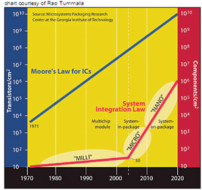
Figure 2 Functional or component density timeline for SoP mixed-signal system integration (courtesy of Rao Tummala).
In 2006, the Packaging Research Center of Georgia Institute of Technology reported on the use of Si-matched low CTE, high modulus C-SiC composite core substrates to fabricate a SOP4 baseline process test vehicle. The goals of the testbed are to explore optical bit stream switching up to 100 GHz, digital signals up to 5 to 20 GHz, decoupling capacitor integration concepts to reduce simultaneous switching noise of power beyond 100 W/chip, design, modeling and fabrication of embedded components for RF, microwave and millimeter-wave applications up to 60 GHz. The baseline process demonstrated several leading-edge technologies including new processes for low-loss substrate material, high density build-up wiring, embedded RF components and thin film passives, novel interconnects and wafer-level packaging3 shown in Figure 3.

Figure 3 SoP integration of digital, RF and optical functions into a single package (courtesy of Bryan Christie Design).
A semi-additive plating process was used to produce multi-layer “micro-vias” with diameters of 15 to 30 microns. The substrate build-up utilized 10 micron thick benzocyclobutene (BCB) dielectric films with dielectric constant of 2.65 and a low loss tangent of 0.0008 at GHz frequencies. This build-up was achieved without the use of any vacuum deposition or polishing/CMP processes and was also demonstrated using commercially available medium CTE organic laminates. Low cost electroless and electrolytic plating processes using plasma surface treatment were able to achieve 6 to 8 micron line widths and spaces.
SoP/SiP Platforms and Commercialization
SiP and SoP approaches for RF and microwave multi-component modules are being developed on three major substrate platforms: (a) ceramic or LTCC, (b) multilayer organic (MLO) or build-up organic laminates, and (c) thin film on silicon. MLO substrates use an inexpensive substrate such as FR-4 and a low-cost advanced epoxy or other low loss polymers as dielectrics. These substrates are being adopted in high-volume applications well into the GHz frequency range. The key to properly simulating such substrates —especially for digital signals—is an accurate, wideband dielectric model. Such a model must capture detailed frequency-dependent behavior from DC to many tens of GHz. From an accuracy perspective, frequency-independent or other simplistic approximations are problematic across the wide range of frequencies found in today’s digital signaling; a better fit to realistic behavior is required. Yield is also affected by the quite loose tolerances of materials like FR-4. Such effects should be studied by statistical simulations with varying material properties.
Motorola, a founding partner with the Packaging Research Center, uses parts of SoP technology in two models of its GSM/GPRS quad-band cell phones to gain about a 40 percent reduction in board area. The module contains all the critical cell phone functions: RF processing, baseband signal processing, power management, and audio and memory sections. Not only does the module free up space for new features, it is also the foundation around which new cell phones with different shapes and features (camera or Bluetooth, for instance) can be rapidly designed. The company reports it has shipped more than 20 million SoP-based phones.
With the advance of SoP processes and materials, RF components such as capacitors, filters, antennas and high-Q inductors can be better fabricated on a package substrate other than silicon, giving SoP the upper hand over SoC and silicon-based SiP. High-speed, board-level optical interconnects are moving to the package as chip-to-chip, high-speed interconnections replace copper, addressing both the resistance and cross-talk issues of electronic ICs (yet micro-miniaturization re-introduces this issue at the package level). In addition, waveguides, gratings, detectors and couplers can all be embedded in the SoP substrate, allowing SoP to integrate micro-miniaturized electronic and bio-electronic systems, such as nano-bio-sensing elements, control/feedback electronics, display, and RF/wireless components up to and including an integrated antenna. For these capabilities, SoP is emerging around the globe particularly in Japan where the historical chip-centric SoC methodology is frequently replaced with a cheaper, faster-to-market IC-package-system co-design flow.
Embedded RF Passive and Active Components in SoP
SoP and SiP designs partition the passive components to the less-costly board/package. Passives include fundamental electrical components such as inductors, capacitors and resistors as well as passive building blocks including high-performance filters, baluns, couplers and integrated antennas.
Multi-layer Inductors
Perhaps chief among these passives are the inductors that would otherwise take up a lot of expensive real-estate on the ICs. High-Q on-chip inductors are difficult to accomplish because of the high parasitic capacitance of thin film dielectrics, high conductor resistance and lossy substrate. The challenge is to utilize the 3D nature of SoP to produce miniaturized, multi-layer inductors with high-Qs over the required frequency range. One example from 2002 is the CPW spiral inductor, depicted in Figure 4, which avoids via losses, reduces dielectric losses and results in an increased self resonance frequency (SRF). The thick copper metallization in the packaging process decreases the shunt parasitic capacitance and reduces the eddy current flowing in the ground plane, which produces a negative mutual inductance effect, resulting in a Q of 182, SRF of 20 GHz, Leff of 1.97 nH for a 36 mil diameter.7 Ongoing research efforts have led to similar results with much smaller components.

Figure 4 Photograph of multi-layer 36 mil CPW inductor (~2 nH) and performance graph (presented at 2001 IMS).
The PRC has been working in partnership with more than 15 semiconductor and supply chain companies since 2007 on a consortium research program on embedded active and passive components (EMAP). As part of this research, this past year, Rao Tummala, Venky Sundaram and Mahadevan Iyer at the PRC and partners at the Institute of Microelectronics in Singapore, presented a paper, “Ultra High Q Embedded Inductors in Highly Miniaturized Family of Low Loss Organic Substrates” at the ECTC conference discussing for the first time the design and fabrication of embedding ultra miniaturized RF inductors in ultra thin (100 to 150 microns thickness) organic substrates. The substrate described belongs to a new family of ultra low profile organic laminates with a loss tangent of about 0.0034 to 0.0045 and a dielectric constant of 3.4. The innovative design resulted in unloaded quality factors of about 100 to 150 in the frequency range of 1 to 15 GHz using line widths in the range of 2 to 4 mils and occupying an area of 0.062 to 0.64 mm2.
Also this past year, Jacket Micro Devices Inc. (JMD), a commercial provider of embedded passive technology, and a spin-off from SoP technology developed at the PRC, developed a novel method of fabricating multi-layer inductors using its proprietary Multi-Layer Organic (MLO™) and Low Temperature Laminated Organic (LTLO™) processes. Using their technique, JMD has demonstrated Q factors of over 150 at 2 GHz, making them ideal for a wide variety of wireless applications where high Q is critical.
Embedded ICs
The EMAP program has also demonstrated a novel “chip-last” embedded IC technology that overcomes the yield and business model concerns associated with current embedded IC approaches by embedding thinned ICs into a high precision cavity in the organic substrate build-up layers using standard flip-chip assembly methods (see Figure 5).
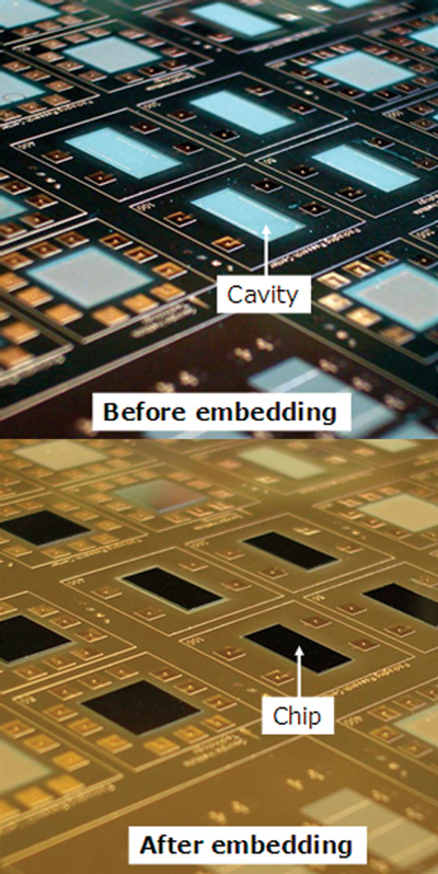
Figure 5 Chip-last embedded IC in organic substrate cavity demonstrated by the PRC EMAP Consortium.
Embedded Decoupling Capacitors
A thin film technology based on barium titanate (BaTiO3) epoxy polymer nanocomposites has been developed to manufacture high performance embedded capacitors. The technology is able to produce high capacitance density (10 to 100 nF/inch2), large area, thin film capacitors (see Figure 6) with controlled thickness from about 2 to 25 microns for a series of BaTiO3 epoxy nanocomposites. The SoP test vehicle from the PRC demonstrated embedded decoupling capacitors with capacitance density of > 500 nF/cm2 integrated into the build-up layers using synthesized BaTiO3 thin films that were deposited on copper foils and integrated using vacuum lamination and subtractive etch processes. The loss tangent of the films was measured to be 0.03 at 100 MHz. The electrical properties of capacitors fabricated from BaTiO3-epoxy nanocomposites showed a stable capacitance and low loss over a temperature range of 25° to 100°C. The capacitance change was less than 10%.

Figure 6 Cross-section of embedded capacitors.
Embedded High Q RF Capacitors
Current and future RF designs require a capacitance density of above 100 nF/cm2, Q of greater than 200 and high tolerance. In addition, the capacitance value has to be stable within 0.3% over 100°C range of temperature to meet the performance requirements. Current organic-compatible embedded capacitor technologies such as epoxy-based composites with ceramic fillers (shown in Figure 6) are not suitable for high performance microelectronic devices such as embedded RF capacitors with high Q and low temperature coefficient of capacitance (TCC) requirements. They may not achieve dielectric loss less than 0.02 and TCC within 300 ppm/sq, even with the best ceramic fillers. RF capacitors from low loss polymers such as liquid crystal polymer (LCP), bisbenzocyclobutene (BCB) and poly tetrafluoro ethylene (PTFE) are being pursued; however, they are limited in capacitance density due to the low dielectric constant polymers.3-4
Nanostructured ferroelectric and ferromagnetic materials show superior dielectric and magnetic properties from superior exchange coupling between the domains, absence of leakage, smaller relaxation time for dipole switching, absence of domain wall assisted relaxation, etc. These materials show superior microwave properties and can be processed at organic compatible low temperatures leading to low cost microwave device integration. A new set of high k paraelectric particles have been investigated by PRC to enhance the RF performance of polymer composites.5 These composites have permittivity of 10 to 20 while meeting the TCC and loss requirements, which can be further enhanced with the nanostructured ferroic materials. For RF capacitors based on inorganic thin films, PRC also pioneered low temperature processes to integrate pyrochlore based barium and strontium titanium oxides that are reactively grown by solution chemical treatment and oxygen ion irradiation at organic compatible temperatures. These high k phases have higher permittivity than silicon oxynitrides or tanatalum oxide capacitors while meeting other microwave requirements. For emerging microwave applications, PRC is developing novel nanocomposite formulations to further enhance both the permittivity and permeability at GHz frequencies. Nanocomposite technology, coupled with metamaterial designs, can lead to small microwave components leading to complete system integration.
Resistors
The PRC test vehicle demonstrated two methods of manufacturing embedded thin film resistors in the substrate. Thin metal alloy resistor films were integrated into the SoP substrate using NiCrAlSi thin films (25 ohms per square) deposited on copper foils (Gould Electronics) laminated on the build-up layers with a two-step etch process for resistor definition. The researchers also used an electro-less plated Ni-W-P thin film (resistance values ranged from 70 ohms to a few kilo ohms per square) on the BCB dielectric by plasma surface treatment and activation. The process was reported to exhibit uniform resistor thickness in the sub-micron range, offering a low profile and excellent adhesion to BCB dielectric while providing a potential seed layer for any subsequent direct electroplating of copper traces. The process was also compatible with the package substrate manufacturing infrastructure.6
Part II: Design Considerations
According to Hee-Soo Lee of Agilent Technologies, critical issues such as wideband and low-loss interconnects, high-Q multi-layer passives including R, L and C, board-compatible embedded functions (antennas, MEMS), low-loss and low-cost boards, efficient partitioning of MMICs, low-cross talk single-moded packages, as well as design rules for vertically integrated transceivers are among the issues that have to be addressed accurately over a very wide frequency range. In addition, there exists a significant gap in the area of hybrid CAD needed to model novel functions that require fast and accurate modeling of electromagnetic, circuit, solid-state, thermal and mechanical parameters. Full acceptance of RF-SoP requires cost effectiveness and reliability, features which are being addressed by the RF EDA community.
Mentor Graphics’ Viklund states that his company sees little difference between MCM, SiP and SoP. Their customers did stacked die MCMs with thin film passives many, many years ago before anyone even dreamed up the acronym SoP. Viklund comments, “Companies use the technology necessary to get the job done and this means that sometimes an MCM suffices while the next design would qualify as a SoP. The need for embedded thin film passives in the substrate varies from design to design within the same company so Mentor Graphics talks about ‘Advanced Packaging Tools’ having all the capabilities needed to meet the varied design challenges our customers are facing today.” That said, multi-layer embedded passives are a specific technology that requires specific EDA support to be viable.
When embedding ICs, an EDA flow is required that can place parts on inner layers and manage unique sets of manufacturing documents for each placement layer. In addition, parts have to automatically drop into cavities without having to build special versions of the library. It also offers challenges to the 3D wire bond and parts Design Rule Checking (DRC). As mentioned, DRC has to be real-time and with parts on inner layers, it becomes so much more critical that the tool directs users to follow the design rules.
For example, Mentor Graphics’ embedded passive technology manages the entire design flow from material parameters, manufacturing process related parameters to automatic synthesis of passive thin and thick film components and real time DRC helps ensure first turn success. In this flow, simulation and analysis are vital components, initially as early planning tools, but as the design is getting closer to completion, a gradual transition from first-level simulation to full electro-magnetic analysis. Shortcuts in this process are known to cause re-spins and current simulation integrations allow very fast and seamless data transfer between design and simulation to make it practical to run simulations whenever needed.
Interconnect and Embedded Passive Modeling
The complex and highly dense nature of SoP embedded passives and interconnects lead to parasitics that will limit the performance unless adequate steps are taken via co-design. For instance, the serial inductances as well as mutual capacitances have a serious influence on the signal quality. In particular, they affect the signal’s shapes and lead to crosstalk problems, which are best predicted using a full 3D field simulation such as Ansoft HFSS, CST MICROWAVE STUDIO® (CST MWS) (see Figure 7 or EMPro from Agilent). Both can analyze these complex structures and deliver information in both the time and the frequency domains (S-parameters), each offering different approaches to circuit co-design.

Figure 7 3D EM model (HFSS) of SiP interconnects and vias, courtesy of Ansoft LLC and Skyworks Solutions (a), and SiP model with port definitions for CST transient simulation, courtesy of CST and AET Japan Inc. (b).
What are some of the simulation issues with using these materials and high-density multi-layer substrates? Agilent’s How-Siang Yap states, “The frequency domain linear simulation technology that produces S-parameters was the primary simulation technology for conventional RF/MW circuit designs. The analytical circuit models such as microstrip, stripline, and co-planar are extensively used in the simulations; however, it assumes the physical structure to be simulated must be as close as the structure modeled, for example ground planes and enough spacing to other adjacent traces. Due to the smaller form factor for high volume applications, it is practically impossible to avoid the parasitic behavior of multilayer designs. The two most important simulation issues in the multilayer designs are the inclusion of imperfect grounding effects and coupling due to the proximity between parts to parts and traces to traces or even for traces to the ground planes. All of these can be addressed by brute force complete EM simulations. Nevertheless, the ultimate design challenge from multilayer circuit designers’ standpoint will come from how to pin-point the source of the problem area. The reason is because the traditional EM simulation only provides final results on whether the structure is working or not (black box S-parameters). A more elegant technique called Coupling Analysis, pioneered by Agilent EEsof EDA, enables different combinations of suspect coupling structures to be simulated by including or excluding certain objects and setting up different coupling distances, and the resultant S-parameters and visualization of current field plots provide a way to identify the impact of parasitic behavior (loss, coupling, radiation, etc.) AND where it is occurring so that the designer can fix it.”
With so many buried and embedded components, what seems to be the most practical ways for an engineering team to achieve successful integration of multiple die, passive on-board components and interconnects into one module? After working closely with their design customers, the application engineers at AWR feel that, “You have to partition the circuit into workable sub-circuits that lend themselves to a top-down, parametric design capability as far into the product development cycle as possible. Once the initial topological selection is performed for complex circuits like MCM or SoP, the designer often switches to an analytical, bottom-up design style based more on EM solvers than on parametric circuit simulation. The design team can forego concurrently designing the coupled sub-circuits if the partitioned sub-circuits can be designed independently. That is, it can be performed by representing their coupling to other sub-circuits or parasitic design elements as definable parametric elements (non-ideal harmonic loads or lumped/distributed models), respectively.”
Both AWR and Agilent felt the ultimate solution for passives and interconnects is the full module verification via EM simulation; however, this only makes sense for final design verification due to the extremely time consuming simulation processes. According to AWR, “The entire design ultimately must be verified electrically via EM simulation and for manufacturing via DRC, LVS and DFM. If the team has thoroughly explored the design before verification to understand couplings and sensitivities, it may not be necessary to place the entire design into an EM solver for verification. Instead, the SoP or MCM design can be electrically verified by selective EM analysis. However, it is essential to conduct parametric exploration of the circuit throughout the design process to gain an understanding of the critical dependencies, sensitivities and couplings.” Agilent concurred, stating, “A more practical approach for an engineering team is a piecemeal approach but brings all of them into co-design platform for analyzing and optimizing the dynamic interactions between them. To speed up the passive circuit design process for the piecemeal approach, the technique that builds parameterized scalable EM models for passive structures based on accurate EM simulation using the patented technology called Multi-dimensional Adaptive Parameter Sampling (MAPS) technology of AMC (Advanced Model Composer) can be also used.”
Layout and Design Rules
To adequately simulate some of these structures, it is important to go beyond simulation itself and look at the entire design. The SoP structures are most often layout-driven, so to adequately simulate them, you need a seamless flow from layout to simulation. How is multi-layer passive component design and embedded ICs changing the requirements for CAD automation? According to Mentor Graphics, multi-layer embedded passives are specific technology that requires specific EDA support to be viable.
According to Agilent, the CAD requirements for the physical implementation are: a) unified stack-up; b) connectivity support; c) electrical rule check (ERC); d) design rule check (DRC); and e) assembly rule check across chip, module and board. For simulation, an example is moving large spiral inductors off an RF chip to become an embedded multi-layer component to reduce the cost of semiconductor area used. The impact on CAD automation means that it now has to support co-design of the chip and module with simulation to accurately account for the 3D interconnects such as wire bonds or solder-bumps along with the embedded active system or circuit ICs. Co-design requirements necessitate the tight integration of system, circuit and 3DEM simulators under the same co-design platform. Standalone 3DEM tools cannot support this kind of flow.
According to AWR, engineers really don’t want to abandon parametric, top-down design because they have a great deal of comfort with the approach as no one actually wants to repeatedly move lines and/or resize components and then run EM simulation for half a day. With this in mind, AWR has developed new technologies specifically designed to solve this problem. For example, EXTRACT is an automated, schematic-driven EM capability that lets users use the schematic- or layout-driven parametric approach to design, but does not require them to manually run the EM solver and then stitch back the resulting, high pin-count S-parameter block into the schematic.
Is the EDA associated with SiP or SoP design evolving in a way similar to IC or SoC design with regards to design kits, LVS and DRC? According to Mentor Graphics’ Viklund, “This is a classic question. Still, the challenges in SiP and SoP design are unique and do not lend themselves to borrow methodology from other technology. Clear, however, is of course that design kits, which really are just protected templates of proven technology, are being used both to save time and to mitigate the risk of errors. In terms of LVS and DRC, the keyword in SiP design is “real time DRC” and this is true even for 3D related physical and manufacturing rules. It’s simply too late to find errors using batch LVS and batch DRC processes even though the batch checks are used as a final sign off process.”
Agilent’s How-Siang Yap pointed out the difference between IC design flow and those required for SoP design. “As we discussed in the previous questions, more challenges exist in multiple technologies used in SoP than IC or SoC designs. Therefore the EDA technology is evolving more to the co-design concept which can be divided into front-end co-design for simulation perspective and back-end co-design for layout/assembly/packaging perspective. For the front-end co-design, the trend is in the integration of different simulation domains into a single unified design platform which can be called high frequency and high speed co-design platform. For the back-end co-design, the trend is in the integration of different back-end tools which has different technology files and design/assembly rules.”
AWR more or less agreed, while adding, “SoP design is evolving this way in the sense that each IC and packaging technology has a PDK or design kit with LVS, DRC, and support for AWR routing and interconnect technologies such as bridge code automatic via insertion and iNet automated routing. The same demands are being placed on laminate and IC kit development, and perhaps even more as these technologies can be concurrently co-designed, co-simulated, and co-verified within the AWR UDM. However, it is not evolving this way in the sense that the integrating technology is PCB-based and not IC-based. The company sees a tremendous demand for simultaneously running real-time PCB DRC and using PCB DFM while still verifying RF and microwave electrical performance at the circuit or system level. The Agilent Mentor DA and AWR Connected for Mentor Graphics Expedition flow supports real-time integration so that the PCB aspects are being altered in the DRC context while the electrical characteristics are simultaneously verified to ensure that performance has not been sacrificed. This is all performed at the parametric, circuit, or system level without reducing the design to ‘dumb metal’ and just subjecting everything to EM simulation.”
CAD data and simulation data (structure geometries for EM) are not necessarily compatible. So, what is the state-of-the-art in sharing information between the CAD group and electrical design group from the perspective of sharing information between environments? Agilent responded by stating that, “Yes, it is true that CAD data and structure geometry data for EM are not necessarily compatible. One example is via holes. Via hole in CAD data format is true representation of physical structure, for example very small arc resolution for circles. However, the required via holes in EM simulation don’t have to be that complex since it creates more simulation burden without improving the accuracy of simulation. The state-of-the-art for design flow integration is intelligence of CAD data translation process. As demonstrated in Agilent EEsof EDA design tools, the via holes from the CAD environment can be simplified into rectangular or polygonal vias for faster EM simulations without manual CAD manipulation. Also it is important to automatically import substrate stack-up information without manual intervention.”
IC Modeling
Multi-chip devices also contain active devices and ICs that need to be accounted for in the design process. What level of MMIC and RFIC model detail is necessary and available (in the case of vendor supplied die) for designers simulating a multi-chip module? Often, there is insufficient data being supplied at this level. According to Agilent, “The most accurate model available with full IP protection is the X-parameter model and can be generated by measurement with Agilent NVNA or simulation with ADS. X-parameters are the mathematically rigorous extension of S-parameters to fully capture nonlinear behavior that includes frequency conversion and impedance mismatched harmonics of cascaded nonlinear components. When measured or simulated with load pull termination, the X-parameter models are valid across a wide range of terminating impedances. Today, measurement-based X-parameter models are limited to two ports due to available hardware instrumentation, but simulation-based X-parameters can be generated for multi-port non-linear components such as mixers and transceivers. Early beta customers representing IC design houses and major handset vendors are fully embracing X-parameter models because it provides a compact accurate language to communicate and simulate nonlinear behavior of MMIC, RFIC, PAM and FEM between design partners.”
AWR sees additional complexity to the problem: “Many MMIC and RFIC customers have to do their own application-specific testing and then use the results at the SoP or system level. The problem is very complex because the loads presented to some of these ICs are not normally characterized by IC vendors. Compounding this, because of the small form factor of the SoP or MCM, is die-to-die coupling. Once you have couplings that cannot be represented at the boundary of a die, you need a circuit-level description of the die to get at some of these problems. A behavioral or compact model of the die is no longer adequate.” Furthermore, multi-chip co-design may likely call for analysis in both time and frequency domains.
Conclusion
Multi-chip design is an evolving technology that offers faster time-to-market and lower development costs compared to single IC solutions yet can still deliver functionality and reduced size. SoP is the leading multi-chip technology today, whereby embedded passive components are approaching the 1000 components per square centimeter milestone. As process technology transitions from the micro to nano scale in the 2010 timeframe, SoP will deliver more capability in ultra-miniaturized packages. This development must occur hand-in-hand with increased capabilities in EDA design flows and simulation technologies as well as a growing knowledge of how to address the complexities of IC/package co-design among engineering teams.
References
1. R.R. Tummala, M. Swaminathan, M. Tentzeris, J. Laskar, G.K. Chung, S. Sitaraman, D. Keezer, D. Guidotti, R. Huang, K. Lim, L. Wan, S. Bhattacharya, V. Sundaram, F. Liu and P.M. Raj, “SoP for Miniaturized Mixed-signal Computing, Communication and Consumer Systems of the Next Decade,” IEEE Transactions on Advanced Packaging, pp. 250-267, May 2004.
2. K. Lim, et al., “RF-System-on-Package (SoP) for Wireless Communications,” IEEE Microwave Magazine, March 2002, pp. 88-99.
3. www.rogers.com, www.gore.com, www.oakmitsui.com, www.dupont.com.
4. D.C. Thompson, J. Papapolymerou and M.M. Tentzeris, “High Temeprature Dielectric Stability of Liquid Crystal Polymer at mm-Wave Frequencies,” IEEE Microwave and Wireless Components Letters, Vol. 15, No. 9, 2005, pp. 561-563.
5. J.H. Hwang, P.M. Raj, I.R. Abothu, C. Yoon, M. Iyer, H.M. Jung, J.K. Hong and R. Tummala, “Temperature Dependence of the Dielectric Properties of Polymer Composite-based RF Capacitors,” Journal of Microelectronic Engineering, November, 2007.
6. V. Sundaram, R. Tummala, et al., “Recent Advances in Low CTE and High Density System-on-a-Package (SOP) Substate with Thin Film Component Integration,” Proceedings of the 56th IEEE ECTC Conference, San Diego, CA, June 2006, pp. 1375- 1380.
7. M.F. Davis, S.W. Yoon, S. Mandal, M. Maeng, K. Lim, S. Pinel, A. Sutono, J. Laskar, M. Tentzeris, T. Nonaka, V. Sundaram, F. Liu and R. Tummala, “RF-Microwave Multi-band Design Solutions for Multilayer Organic System on Package Integrated Passives,” 2002 IEEE MTT-S International Microwave Symposium Digest, 2002, pt. 3, Vol. 3, pp. 2217-2220.