
High power RF amplifiers are expected to provide high primary performance parameters such as output power, gain and efficiency, as well as operate reliably for more than 20 years in the field. Traditionally, designers have built these amplifiers using components fabricated in cost-effective silicon-based technologies such as bipolar or LDMOS. While these technologies can operate at high voltages, they suffer from low ruggedness ratings. For example, LDMOS has an inherent destructive mechanism (i.e., a parasitic bipolar transistor) built into the transistor structure that limits the ability of the device to work reliably at high operating voltage. In contrast, the HVVFET exhibits extreme ruggedness in high voltage, high power and high frequency wireless applications.
Defining Ruggedness
Ruggedness refers to the ability of the RF power transistor to withstand load mismatch conditions under high output power conditions without experiencing device failure or measurable long-term degradation in device performance. Under mismatched load conditions a large amount of power can be fed back into the active device where it is dissipated in the semiconductor. The ability to handle the large power dissipation internally in the active area without altering the performance is indicative of a reliable device.
Although there are no standard metrics to uniquely define ruggedness, the ruggedness of a specific transistor will be a function of the magnitude and phase of the mismatch, the output power level conditions and the thermal dissipation properties of the amplifier. Similarly, no widely accepted standard exists to define the input conditions or the pass/fail criteria for ruggedness testing. However, catastrophic device failure is always a ruggedness failure.
Some semiconductor device manufacturers define the failure criteria for the ruggedness test as zero degradation in output power. This is not an adequate definition for failure, however, since some technologies, like bipolar, can deliver the full rated output power even when the ruggedness test damages some of the cells so that the remaining cells provide the full power at a higher temperature, which will result in a decrease in the MTBF of the device. Other power device manufacturers specify failure criteria as a more than 20 percent shift in one or more of the DC test parameters.1 A few semiconductor power device vendors do not specify a ruggedness rating at all. Some LDMOS manufacturers measure ruggedness with what they call a ‘burn-in’ test. The ‘burn-in’ test acts as an accelerated life test, causing a large change in the DC parameters after a single trial that minimizes the performance drift over the operating lifetime of the active device in the field. The following discussion will describe a comprehensive ruggedness test. Using data collected in this test, this article will demonstrate that this new high voltage vertical technology does not exhibit any measurable performance difference before and after the test.
Critical Metric

Figure 1 Transmitter diagram with antenna.
Ruggedness is among the most important reliability metrics for high power amplifier designs. Figure 1 shows the block diagram of an RF transmitter chain. In a communication system, the information to be transmitted is processed in the baseband using DSP and analog logic circuits. In order to transmit this information in an efficient manner the data is modulated with an RF carrier frequency. The local oscillator is used to mix the required information up to the RF frequency. The power amplifier (or power amplifier chain) transmits this signal into the air through the antenna with the output power of the final stage amplifier and the antenna gain determining the range that the information is broadcast. A power amplifier output matching circuit transforms the output impedance of the transistor to the antenna impedance in order to optimize the performance of the active device. The antenna component, however, is exposed to uncontrolled environmental conditions so that the antenna impedance will vary. Similar issues affect radar transmitter ruggedness.
Superior ruggedness can also reduce cycle time during the initial circuit design process. Once high power amplifier design moves from theory to the laboratory bench, much of the procedure involves measuring amplifier characteristics while modifying the matching circuit of the device. When a design involves a device with low ruggedness, engineers must use extreme care in these experimental matching circuit trials in order to avoid damaging the device. A highly rugged device, however, allows the designer to move more quickly to optimum conditions without fear of device damage or destruction.
Measuring Ruggedness

Figure 2 RF bench diagram with load and line stretcher.
Figure 2 shows a standard RF bench and the equipment needed to measure the RF performance of a power amplifier. During device characterization an industry standard matched load of 50 ohms is presented to the output of the power amplifier. When performing the ruggedness test, the RF switch changes the load from the matched case to that of a shorted load connected to a line stretcher. The line stretcher component varies the phase of the shorted load over a full 360 degrees simulating the conditions that can occur in the real world application.
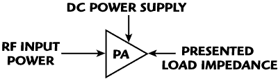
Figure 3 Parameters affecting power amplifier performance.
There are three controlling electrical factors presented to the power amplifier in a ruggedness test, which are the amount of input power, the DC bias supply voltage and the load presented to the device, as shown in Figure 3. A fourth factor, temperature, also can affect ruggedness, but is first order independent of the three electrical factors, so is not considered in the following discussion. Any of the electrical factors can be varied, although many semiconductor vendors only vary the mismatch seen by the load and use the nominal value for RF power and bias voltage. The semiconductor may indeed prove rugged under these set conditions. However, a true test of ruggedness will vary all of these factors at the same time to accurately mimic real world conditions and see if the device still maintains performance after the ruggedness test. “A truly realistic possibility... is the condition whereby the RF power device ‘sees’ a worst case load mismatch (an open circuit, any phase angle) along with maximum Vcc and greater than normal input drive—all at the same time.”2
The HVVFET technology exhibits the capability to survive a ruggedness test that presents 1) an input power level twice that needed to obtain rated output power; 2) a bias supply voltage that is 10 percent greater than rated power supply level; and 3) a mismatched load that is the highest in this industry. The device can survive this extreme condition and show no degradation in performance after the ruggedness test.
Under linear conditions, a perfectly matched load is able to convert the entire applied RF signal into transmitted RF energy. A mismatched load will transmit some of the RF signal, but will reflect the remaining power back into the device. This reflected power must be absorbed internally in the transistor. The amount of energy reflected is measured by the reflection coefficient, gamma, where the magnitude of gamma normalized to unity relates to the amount of reflected energy (i.e., gamma of zero implies no reflection and perfect transmission, while a gamma of one implies total reflection). Another parameter that expresses the amount of reflection and characterizes the type of mismatch is the voltage standing wave ratio (VSWR). It is directly related to the magnitude of the reflection coefficient as seen in Equation 1.


Figure 4 VSWR vs. gamma.
VSWR is the more common figure of merit when discussing ruggedness testing. The higher the VSWR, the more power that is reflected back to the load of the amplifier. That power must be absorbed by the active device without damage. As you can see in Figure 4, a VSWR of 5:1 implies that nearly half of the desired output power is actually reflected back to the amplifier and a VSWR of 10:1 corresponds to more than 2/3 reflected energy. Most semiconductor companies specify the ruggedness of their devices with one of these two VSWR conditions. The measure of the robustness of the vertical device is its ability to pass a ruggedness test with a mismatch of 20:1 VSWR, which reflects more than 85 percent of the output power back into the device under test.
Creating VSWR
During a ruggedness test a load with a certain VSWR is presented to the device and the phase of this load is varied over an entire period. The phase of the load is modified by a line stretcher (see Figure 2). Different values of VSWR are obtained by using a short circuit, having a magnitude of reflection of 1, and an attenuator. A lossy coaxial stretch of line acts as the attenuator. An infinite VSWR is achieved by terminating the load with a short and no attenuation. Note that the 20:1 VSWR is achieved by connecting the short directly to the line stretcher, which is effectively a zero line length. Real world losses in the output coupler, RF switch and line stretcher attenuate the magnitude of the reflection coefficient by a few percent generating a VSWR greater than 20:1, but less than the theoretical value of infinity. Varying the length of coaxial cable will vary the VSWR presented to the load. The shorter the coaxial cable length, the smaller the attenuation, producing higher VSWR. The length of the cable is determined by the properties of the cable, the desired VSWR and the frequency of interest. Three different VSWR values are achieved using different line lengths, as seen in Figure 5. Theoretically, the VSWR will present a perfect circle on a Smith Chart as it is rotated through all 360 degrees of phase. In the real world, however, there are losses in the coaxial cable and therefore the VSWR is expected to change as the line stretcher varies the phase of the device through all 360 degrees. This effect is seen in Figure 5 as the 10:1 VSWR line presents a minimum of 10:1 VSWR across all phase angles. This is true of all line lengths and for all future references a VSWR of 20:1 implies a minimum VSWR of 20:1. In many cases it is actually much higher than the stated value.

Figure 5 VSWR vs. line length.
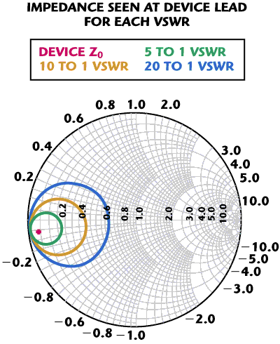
Figure 6 Impedance Smith Chart vs. VSWR (sweep min. 1060 MHz).
Figure 6 depicts the impedance presented at the leads of the device as the phase is swept from 0 to 360 degrees for each VSWR condition. As the phase is varied, the device sees the impedance indicated by the VSWR circle. Generally, when the impedance is less than the nominal impedance and under an ideal load, the device will operate in a low voltage/high current condition. If the high current generates enough heat, thermal failure can occur due to the silicon melting. If the impedance presented to the device is greater than the nominal impedance, the device will operate in a high voltage/low current situation. When the high voltage condition exceeds the breakdown voltage rating, the device goes into avalanche breakdown.
Operating Voltage Considerations
The vertical MOSFET technology allows the epitaxial layer to standoff a large amount of voltage. The higher drain-source transistor breakdown voltage gives the transistor the ability to withstand high voltage spikes on the drain without damaging the device. Typically under normal operation, RF power transistors are exposed to twice the voltage swing of the operating voltage as the AC signal rides on top of the DC bias voltage. This condition is observed even under ideal conditions of nominal DC supply voltage, input power and a load matched to 50 ohms. There are instances in the normal operating life of the power transistor when all of these three factors change to a non-optimum condition. There are times when the load condition is mismatched from the ideal 50 ohms to an open load with any given phase angle. The general rule of thumb in the industry is that the mismatched load impedance condition will create voltage swings on the load of approximately 2.5 times the rated DC power supply voltage. Since the HVVFET breakdown voltage exceeds 115 V, it supports operating voltages of 48 V.

Figure 7 Voltage walk-out.
In addition, the HVVFET can handle a large avalanche current without overstress to the device. The limitation on the avalanche current in the HVVFET is that the avalanche power (the product of breakdown voltage and the avalanche current) be less than the maximum power dissipation rating of the device. In the case of this device, the maximum power dissipation calculated with the thermal resistance is 875 W. Therefore, with breakdown voltage equal to 115 V, the maximum allowable avalanche current is 7.6 A. This high avalanche current rating allows the HVVFET to survive severe over voltage ruggedness conditions with a low operating voltage to breakdown voltage ratio. Figure 7 shows the behavior of the HVVFET breakdown voltage versus temperature. The positive temperature coefficient means that the high avalanche current condition will not result in destructive thermal run away. As the device temperature increases due to an avalanche condition, the breakdown voltage increases thus limiting the amount of avalanche current. This characteristic allows the transistor to withstand high currents and thus higher temperature even at high voltage without damaging the device. Although other silicon technologies such as bipolar and LDMOS structures can operate at high voltages, they only provide ruggedness ratings of 10:1 VSWR or less.
There are many benefits to operating power amplifiers at high operating voltages. First, higher operating voltages lead to higher impedances of the device, which comes from Ohm’s law. The higher device impedance is inherently easier to match than lower impedances and results in fewer matching components and a smaller PCB. This results in a more cost-effective solution.
At any given power level a high operating voltage requires a lower current level. From Watt’s law, the higher power is achieved through either voltage or current.
The advantage of obtaining higher power through voltage is the resultant lower current. Reduced current density reduces all energy-dependent aging mechanisms that lead to reliability issues. Lower current relates directly to higher reliability by preventing metal migration and achieving higher MTBF. Another advantage of the use of high voltage is the higher impedance required for the optimum load of the power transistor device. Higher impedance makes the device easier to match to the industry standard 50 ohm load. The higher impedance requires less current to achieve the same power levels and generates less heat during normal operation.
A third advantage of higher operating voltage and lower current is lower dissipated heat. RF performance parameters such as gain and efficiency decrease as temperature rises. Therefore, heat is the number one enemy of power transistor designers.
The HVVFET uses a 48 V supply, which is over 150 percent the level of typical high power amplifiers that utilize 28 V supplies. This translates into a nearly 3x improvement in the dissipated power consumption that the transistor has to withstand. An RF amplifier with 50 percent efficiency converts only half of the total power in watts consumed from the DC supply into usable transmitted RF power. The other half of the DC supply power is wasted energy that must be disposed of in some manner. The excess power that cannot be converted into usable RF energy is dissipated in the form of heat in the output resistance of the silicon device. The less heat the device generates, the more likely it operates at a safe level and avoids thermally-related failure conditions.
Thermal Considerations
One of the big advantages of vertical technology is the ability to get the heat out of the device rapidly and efficiently. The vertical technology’s improvement in the layout of the active area is designed and optimized for thermal performance. Maximum heat is generated in the drain of the device within a few microns of the gate-source junction and, given the vertical nature of the device structure, the heat travels less than 10 microns through silicon to reach the heat spreading capability of the metalized source contact. Therefore, the thermal path in a vertical device structure is an order of magnitude shorter than other silicon MOSFET technologies. Figure 8 displays the thermal path of the device and demonstrates that the hottest spot in the silicon is, indeed, physically close to the heat sink. This design allows the device to more easily transfer heat to the heat spreading capability of the package.

Figure 8 Diagram of vertical structure (thermal path).
In contrast, bipolar technology has a positive temperature coefficient where an increase in temperature leads to increased collector current. This leads to a feedback condition, thermal runaway, where the increased temperature increases the current, which creates more heat and thus more current. Bipolar technology attempts to avoid thermal runaway by adding resistors to the emitter area to effectively distribute the heat more evenly and prevent the onset of ‘hotspots’ that may go into thermal runaway. While the emitter resistors do tend to spread the heat, they also lower gain performance. All silicon MOSFET technologies exhibit a negative temperature coefficient. As temperatures increase, the amount of voltage required to bias the device to the same level also rises. If the same voltage is continually applied to the gate, the bias current is reduced, which produces less heat and reduces the temperature, thus stabilizing the device.

Figure 9 Diagram of vertical and lateral structures with parasitic BJT.
As the current state-of-the-art technology for RF power transistors, LDMOS devices can operate at high voltages and high frequencies; however, the technology has an inherent destructive mechanism that destroys the transistor in avalanche mode. Figure 9 shows the simplified cross-section of a LDMOS structure with the intrinsic parasitic bipolar transistor. During the avalanche breakdown condition, this BJT turns on and saturates, resulting in a mode of operation called latch-up. During the latch-up condition the MOSFET creates an excessive amount of current, which generates high power dissipation resulting in thermal runaway and destroying the device in operation. Figure 9 also shows the HVVFET technology and the inherent parasitic bipolar transistor in the structure. Unlike LDMOS technology, the HVVFET structure has the base and emitter terminals of intrinsic bipolar transistor tied together at the MOSFET source terminal effectively creating a two-terminal device such as a diode. Thus, the vertical technology does not experience the failure condition of latch-up under avalanche breakdown.
DC and RF performance
The HVVFET device under test (DUT) is internally matched to bring the impedances up to a practical level to be matched to 50 ohms at the PCB board. All device performance data is generated in an evaluation circuit that is at the 50 ohm reference plane and includes all external matching circuitry losses, which closely resembles the actual losses experienced in a matched, real-world amplifier application.

Table 1 Ruggedness Results Summary at Rated Output Power
The device was tested in a standard RF bench set-up, as described in Figure 2. The device was subjected to a ruggedness test where the input power was set to the amount required to achieve the rated output power, the bias was set at a nominal voltage of 48 V and the load was set to a mismatch with VSWR of 5:1 and swept through all phases. The RF power performance metrics before the ruggedness test were compared to the performance after the ruggedness test. The pass/fail criteria are specified as no measurable performance change in any of the DC or RF metrics. The load was changed to the 10:1 VSWR cable length and re-tested with the ideal load for the baseline data. Table 1 summarizes that the device passed the ruggedness test with a mismatched load as great as 20:1 VSWR. The device was then subjected to an over-voltage condition where the nominal bias supply voltage was increased by 10 percent to 53 V. It was subjected to nominal input power drive and re-tested with all three load VSWRs. Again the device passed the over-voltage condition and the high VSWR mismatch over all phase angles. Next, the device was subjected to twice the amount of input power needed to attain the rated output power, which is 3 dB worth of overdrive. Table 2 shows the device passes this condition at both nominal power supply voltage bias and over-voltage power supply bias.
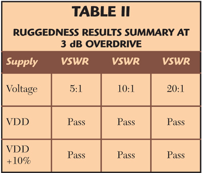
Table 2 Ruggedness Results Summary at 3 dB Overdrive

Figure 10 Graph IDS vs. phase angle.
Figure 10 illustrates the amount of average drain current supplied to the test circuit versus the phase angle of the specified VSWR condition that the device is subjected to during the ruggedness test. If the output power of the device is calculated by Equation 2, it is easy to verify that the average current from the 1:1 VSWR case multiplied by the supply voltage does result in correct output power of the device. As would be expected from Figure 4, there is only an incremental increase in drain current variation as the VSWR is changed from 5:1 to 20:1, but a large increase in drain current variation as the VSWR is changed from 1:1 to 5:1. The effect of drain voltage variation for a fixed input power level shows almost no change in the maximum current. The reason for this is that the device has reached its drain saturation current. This is true for both values of the input drive level. The peak-to-peak variation in the average drain current is greater for the nominal input drive condition than the overdrive condition for the same reason. The device is able to survive the ruggedness tests with no performance changes since the device can handle the maximum current condition, drain saturation, and the maximum voltage condition, drain breakdown, without damage.

Table 3 DC Parameters Before and After Ruggedness Test
The DC and RF data was measured prior to testing as the baseline data for comparison after the ruggedness tests are performed. Table 3 demonstrates that the value of the measured DC parameters of the device do not change by any significant quantity after all the ruggedness tests have been performed. If the ruggedness test was damaging the device, one would expect the DC parameters to shift. Typically ruggedness testing increases Rds(on), decreases Vgs(th) and increases Idss. Table 3 clearly demonstrates that the DC parameters are stable and unchanging before and after the ruggedness testing. Figure 11 displays how the ruggedness testing had no effect on the RF performance of device. The measured RF parameters of gain, efficiency and output power are not affected by the testing procedure as the data after the ruggedness tests lie on top of the data prior to the testing.

Figure 11 Pre/post ruggedness test RF data.
Conclusion
The new high voltage RF power MOSFET described in this article demonstrates a high degree of ruggedness. This new device differs dramatically from traditional bipolar devices that are prone to thermal runaway or LDMOS devices that are susceptible to parasitic bipolar latchup. Moreover, this new silicon vertical technology was able to provide high performance output power, gain and efficiency even after the ruggedness test condition of 3 dB input overdrive and 10 percent over-voltage bias supply line and a 20:1 VSWR mismatched load. By combining this unique trait with better RF power performance, the HVVFET technology offers designers a new opportunity to dramatically improve ruggedness while increasing power density, lowering power consumption and shrinking system size in a wide range of radar and avionics applications.