
The transceiver duplexer is a key element in avionics systems, radars, antenna arrays and wireless communication systems. The duplexer provides protection of the receiver and transmitter from unwanted parasitic signals. This article discusses several duplexer schematics, their development flow and a trade-off design.
Duplexer Schematics
An RF transceiver duplexer connecting a single antenna to the transceiver is often the key component in phase arrays, radar, communications and navigation systems. A duplexer directs the transmitter energy to a single antenna during the transmit mode and the energy received by the antenna to the receiver during the receive mode.
The RF duplexers can be classified according to the timing of the transmit and receive operations: Full duplexer when the transmitter and receiver are operating simultaneously and half duplexer when the transmitter and receiver are operating at different times. In pulse systems, the transmit and receive time are separated. In CW systems (for instance, Doppler radars, CW altimeters, etc.), the transmit and receive modes are implemented at the same time. The duplexer is not a frequency-selective device like a diplexer and must be designed for operation in the frequency band used by the receiver and transmitter.
The duplexers should meet the following objectives:
- reduce the number of antennas (a single antenna for transmitting and receiving)
- reduce the number of cables connecting the transceiver with the single antenna
- reduce the potential transmitter pulling, intermodulation and noise due to antenna mismatch
- protect the receiver from unwanted (parasitic) synchronous and non-synchronous signals
- reduce cost, maintenance and mechanical complexity
The transceiver duplexer has to provide the following electrical performance:
- low transmission loss to maximize the radiated power
- minimum receive loss for low receiver noise figure and maximum receiver sensitivity
- sufficient isolation between transmitter and receiver
- proper impedance match between transmitter, antenna and receiver
- suppression of the unwanted parasitic signals in the receiver and transmitter passes
- high transmitter peak and average power
There are three main types of duplexer in common use. The first duplexer consists of an SPDT transmit/receive (TX/RCV) switch/limiter. The second type includes a ferrite circulator, while the third includes a ferrite circulator and a transceiver protector.
TX/RCV Switch/Limiter Duplexer

Figure 1 TX/RCV switch/limiter duplexer schematics.
Figure 1 illustrates a duplexer that includes a TX/RCV switch/limiter. Practically any PIN diode can be used in a limiter. The main difference between switch and limiter designs is the reflection transients. Several PIN diode switch architecture options should be considered. The most important circuit configurations include: series, shunt or series-shunt PIN diodes. One of the limiters shown includes one shunt switch PIN diode D3 in the transmit pass and two shunt limiter diodes D1 and D2 in the receive pass. The other includes one series switch PIN diode D3 in the transmit pass and two shunt limiter diodes D1 and D2 in the receive path. The shunt diode switches are commonly used for systems with high isolation and are capable of handling higher power because the heat dissipation in a shunt diode (which has one grounded end) is much better than for a diode in a series-type switch due to good heat sinking. Series diode switches are commonly used in broadband circuits. The series-shunt configuration provides greater isolation than the previous version, but requires a bias current from both positive and negative sources that would significantly increase the DC power dissipation.
During the transmit mode, the biased limiter diodes provide active suppression of the synchronous transmitter leakage into the receiver. Also, during the receive mode, the limiter diodes of both schematics provide passive limitation of the unwanted and potentially damaging high-power non-synchronous signals received by the antenna from nearby systems.
The TX/RCV switch/limiter duplexer is characterized by:
- low insertion loss in order to minimize transmitter power delivered to the antenna and receiver input noise figure
- high TX-RCV isolation
- high switching speed
- low harmonic and intermodulation products
- low cost
- small physical dimensions
- good temperature stability
The TX-RCV isolation is achieved by a switch that disconnects either the transmitter or the receiver. The TX/RCV switch/limiter duplexer may not be electrically symmetrical. For example, 20 dB of isolation in the transmit arm is sufficient to prevent any variation in the output impedance of the transmitter from affecting the performance of the receiver, while more than 40 dB of isolation in the receiver arm is necessary to protect the receiver from the strong transmit signal.
A single-stage switch/limiter can typically produce approximately 20 dB of isolation, depending on the PIN diode characteristics. For a greater than 40 dB transmit-receive isolation, multi-stage limiters, such as the two-stage switch/limiter, can be used in the receive pass. The isolation of one shunt PIN diode is given by
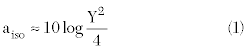
where Y =1/RF is the shunt diode normalized susceptance and RF is the diode series resistance.
For the ON diode mode, the relationship between the isolation of the two-diode shunt-iterated switch and diode resistance RF or susceptance Y can be found1
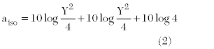
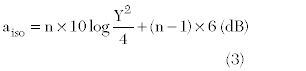
Comparing Equations 1 and 2, it can be seen that the isolation of the two shunt-iterated diodes separated by a spacing of l = λ0/4 is double that of a single device, plus 6 dB (10 log 4) extra. The isolation of an n-diode shunt-iterated SPST switch is
The TX/RCV switch duplexer has the following disadvantages:
- no protection to the transmitter from the transmitter power reflected from the antenna mismatch and from other elements in the TX/RCV common channel
- power-handling capability limit
- switching speed limit
- necessity of control signals
- possible harmonics and intermodulation product
The three quarter-wavelength sections narrow the bandwidth to approximately 10 percent. The operating bandwidth can also be limited by the diode bias network, which is a filter network that isolates the DC bias current from the RF network. To increase the bandwidth and minimize the transmit insertion loss, the distance from the series diode D3 to the common junction should be an absolute minimum. There are different switch modifications with greater bandwidth. The Hewlett Packard network,2 which includes additional transformers with other than 50 Ω impedances, provides a bandwidth greater than 30 percent. Also, to improve bandwidth, a series-shunt diode network can be used.
The conventional narrow-band shunt diode switch topology with quarter-wave diode spacing is too large at low frequencies. A defected ground structure (DGS)3 can provide reduction of size and harmonic signal. A DGS switch shows results very comparable to a conventional switch, in spite of being half the size.
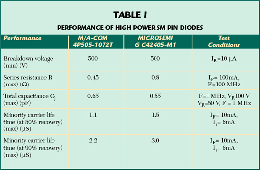
Table 1 Performance of high power SM Pin Diodes
For a good switch performance, the PIN diodes should have a low resistance at low forward current and low capacitance at zero bias. Table 1 illustrates the performance of two high-power surface-mount PIN diodes.
The TX/RCV switch must rapidly disconnect the transmitter and connect the receiver to the antenna. The switching speed limit depends on the PIN diode carrier life time. PIN diode switches can generate harmonics and intermodulation products since PIN diodes are fundamentally nonlinear devices. All distortions are strongly influenced by the lifetime of a PIN diode, as well as the transmitter RF power which is applied to the diode. The contradictory requirements for the switch diode will be discussed later.
Circulator Duplexer

Figure 2 TX/RCV duplexers using circulators

Figure 3 TX/RCV duplexer using a circulator and a transceiver protector.
The duplexers in Figures 2 and 3 include a circulator whose principal role is to protect the expensive, high power, TX RF power amplifier from variation in loading conditions.
The circulator network provides:
- greater maximum power
- no need for electrical switching
- additional attenuation (approximately 6 to 8 dB) to the different harmonics4
In the full duplexer, transmission and reception can occur simultaneously. The main problem is that the isolation of a circulator is poor. Therefore, an antenna mismatch results in poor transmitter-receiver isolation and transmitter pulling due to the signal reflected from the mismatched receiver.
To improve circulator isolation, different options can be used. Dual-junction circulators are used in high-power systems requiring high receive-transmit isolation (up to 50 dB) and transmitter stability. With the isolator installed in the network, any reflected power will flow into the 50 Ω load of the isolator and is dissipated into heat. A three-dimensional dual-junction circulator1 provides a high integration level in the horizontal plane and low cost as compared with traditional multi-junction circulators.
Another circulator duplexer option is a network with a three-port circulator and a transceiver protector that provides:
- greater isolation
- protection of RCV from synchronous and non-synchronous signals
- protection of TX from reflection signal from antenna and other elements in the TX/RCV common channel
- greater maximum RF power
It is possible to maintain high circulator isolation by using an additional compensation network1,5 where the parasitic leakage signal is compensated for by an input signal sample. Emerging new principles and technologies offer possibilities of fabricating low cost nonreciprocal devices without using ferrites. Several designs utilizing an active circulator have been described in the literature.1,6-8 However, these devices possess power handling limitations.

Table 2 Drop-In 3 Port Circulators
These circulators are characterized by:
- insertion loss less than 0.5 dB
- isolation greater than 18 dB
- VSWR<1.3
- peak power handling of 600 W min
Comparison of Different Duplexers

Table 3 Performance of the Three Duplexers
- higher cost
- greater dimensions
- poor temperature performance
- greater insertion loss
- required magnetic shielding
The duplexers with TX/RCV switch/limiter have the following disadvantages:
- no protection of transmitter from reflected synchronous signals
- lower peak power
- required switching control network
Transceiver Protector
The transceiver protector provides:
- protection of the receiver from large input signals while allowing the receiver to function normally when these large signals are not present
- protection of the transmitter from signals reflected from the receiver due to receiver and antenna mismatch
In the duplexer with a circulator, the transmitter power may leak into the receiving system due to non-ideal circulator isolation, antenna port reflection paths, as well as to mutual coupling from adjacent antenna array elements. This can cause such problems as saturation, gain compression of the receiving system and increased FM-AM noise. Any losses between antenna and low noise amplifier (LNA) directly degrade the receiver sensitivity. Also, sometimes unwanted and potentially damaging high-power signals from nearby systems (non-synchronous signals) received by the antenna pass to the receiver. The transceiver protector is primarily used to protect the power-sensitive receiver components and devices (LNA, mixer) from these high-power sources. The transceiver protector can also suppress the unwanted signals reflected from the antenna and the mismatched receiver to prevent transmitter pulling and possible damage. Therefore, the transceiver protector provides protection of both the receiver and the transmitter from the unwanted signals.

Figure 4 Three types of transceiver protector configurations.
There are three types of the transceiver protector configurations,1 as shown in Figure 4. The active limiter works on a separate current source (a). To protect the transmitter from the signal reflected from the active limiter, a non-reflective network can be used. For this network, the terminating impedance is developed by the non-reflective (absorptive) switch including the series combination of the diode and the terminating load to ground. Parasitic signals from mismatches at the antenna and TX leakage are absorbed by the limiter with 50 Ω loads. The required 50 Ω terminating impedance is achieved by the series combination of the PIN diode and terminating resistance to ground. The non-reflective (absorptive) limiter with 50 Ω loads can protect the transmitter from the reflection signals. But in the absorptive switches, the power-handling ability is limited by the ability of the diodes and resistors to dissipate RF power. The active transceiver protector can only protect against signals that are synchronous with the transmitter pulse. Protection against non-synchronous, external signals is provided by the passive limitation of diodes D1 and D2. Absorptive switches exhibit slower switching speed. In some duplexers, the broadband matching is more important than the switching speed.
A duplexer with a circulator and a balanced passive limiter,9 which provides better switching speed performance, is also shown (b). The balanced limiter makes use of the features of two 3 dB hybrids, in combination with limiter diodes placed between two 90° hybrids, to control the power flow. The input splitter divides the input RF signal equally between two limiter diodes. The output combiner recombines the output signals from the splitter. The balanced limiter is a non-reflective network because the reflected signals are dissipated in the input hybrid 50 Ω loads, which prevents transmitter load pulling. The hybrids of the balanced configuration provide a good input and output match at all power levels and a route for the reflected power to the 50 Ω load. The limiter diodes are turned on by the RF signal itself. The passive limiter can include an RF choke inductor as well as a quarter-wave shorted high impedance transmission line. This structure allows a DC signal to pass through, but not an RF signal. In most limiter circuits, DC blocking capacitors are included at the input and the output of the circuit. These series capacitors have low series reactance at the RF frequency and allow to separate the DC current along a transmission line.
A passive limiter is a self-activated switch that is activated by a high-level incident power. The speed of this process depends on the diode lifetime (see Table 1). This relatively slow process leads to a high dissipation power on the diode. The maximum signal RF power that a limiter diode can handle is limited by either the diode’s breakdown voltage or its power-dissipation capability. The absorptive passive limiter usually exhibits somewhat slower switching speeds.

Table 4 Performance of the Three Types of Transceiver Protectors
To eliminate the limiter diode speed problem, a quasi-active limiter (c) can be used. Also, the quasi-active limiter provides both synchronous and non-synchronous protection of the receiver. A two-stage quasi-active limiter with limiter diodes D1 and D2 and two Schottky detector diodes D3 and D41 is shown. The Schottky diodes D3 and D4 are coupled (~20 dB) with the main 50 Ω transmission line through a high-impedance (~120 Ω) transmission line or can be connected through a directional coupler. The limiter diodes D1 and D2 are turned on primarily by the external bias current from the Schottky detector diodes D3 and D4, which are sensitive to the incident signal. Diodes D3 and D4 detect the incident RF power and rapidly apply self-rectified current to the limiter diodes D1 and D2 respectively, causing a rapid increase in attenuation and protection from synchronous and non-synchronous signals. The first Schottky diode D3 starts activating the first high-power limiter diode D1 at approximately 15 dBm incident power. Diode D1 is used as a prelimiter of the high-incident RF power. The second low-power limiter diode D2 has a faster response and, therefore, provides protection during the initial stages of pulse rise time. The parasitic signals reflected from the limiter are dissipated in the dual-junction circulator 50 Ω load. This network prevents transmitter load pulling and leakage of unwanted high RF power to the receiver. Table 4 illustrates the performance of the three transceiver protectors.
Duplexer Development Flow

Figure 5 Duplexer development flow.
Figure 5 illustrates the ANT/TX/RCV duplexer design flow. The system level specification is the first step in a duplexer design flow. The second step is the transformation of system level specification into the duplexer requirements. Some duplexer requirements should be similar to the system requirements; for example, frequency range, maximum power and temperature range. Other duplexer requirements are specific to the duplexer and depend on system requirements; for example, TX and RCV pass insertion loss, TX-RCV isolation and RCV-ANT isolation.
Analysis of RF duplexer requirements (third step) includes the definition of fixed and variable characteristics. Fixed duplexer characteristics are similar to the system requirements and include center frequency, bandwidth, power, etc. The variable duplexer parameters may be flexible and depend on system requirements, performance of other subsystems and devices, and physical implementation of the duplexer network. The variable duplexer characteristics are insertion loss, isolation, matching, cost and size. A designer has to choose the weighting coefficients ki for each duplexer parameter to provide multi-parameter optimization.
The fourth step is the selection of a prototype schematic according to duplexer requirements, analysis of the schematic and the optimum topology trade-off design. After that, the layout can be prepared. The fifth step includes selection of elements (parts), topology and technology process. The sixth step is the detailed design phase that includes calculation and simulation over the specified temperature range and manufacturing tolerances. The final steps (8, 9 and 10) are preparation of documentation, fabrication and evaluation to specification.
Analysis of the duplexer includes multi-parameter optimization for the following major characteristics:
- TX Insertion Loss (IL)
- TX-RCV Isolation (ISO1)
- RCV-TX Isolation (ISO2)
- Matching (VSWR or Return Loss RL)
- RCV and TX protection
- Cost (C)
- Volume (V)

Figure 6 Circle diagram of the duplexer parameters.
Figure 6 illustrates the circle diagram of these parameters with goal values (green) for the two options: 1) SPDT TX/RCV switch shown in brown and 2) circulator with transmitter-receiver protector shown in blue. To optimize the duplexer network, the area between real and goal performance should be minimized. The comparison of the two networks using the circle diagram showed that the SPDT TX/RCV switch corresponded to a smaller area and, therefore, a better performance than the circulator with transmitter-receiver protector. These preliminary results should be corrected using the weighting coefficients for each parameter. A designer has to choose the weighting coefficients ki for each parameter from k=1 (most important) to k= max (least important). The circle diagram should be corrected by using different scales for each parameter according to the weighting coefficients and final decision about the optimal network should be based on a new circle diagram.
Duplexer Trade-off Design

Figure 7 Different duplexer trade-offs.
The most contradictory duplexer parameters include (see Figure 7):
- loss vs. isolation, power, volume and cost
- isolation vs. frequency band
- size vs. power, cost and bandwidth
- electrical performance vs. temperature range
The most important electrical parameter of the transceiver duplexer is insertion loss (IL). The trade-off design can satisfy contradictory parameters: insertion loss versus volume. The integration quality of these two parameters is characterized by the insertion loss – volume integration index:1
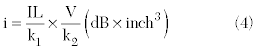
where IL is the total insertion loss in dB, k1 is the weighting coefficient of the insertion loss, V is the volume in inch3 and k2 is the volume weighting coefficient. The optimum duplexer has the minimum integration index imin, which means the smallest physical dimensions and the minimum insertion loss. It is important to keep in mind that the integration index varies linearly with frequency.
Size (volume) of the duplexer depends on electrical requirements, transmission line type, dielectric substrate parameters, component dimensions and the structure of the duplexer. The integration strategy of a duplexer is based on the optimum schematic and design. A number of different transmission lines are generally used in RF and microwave integrated circuits. The trade-off design showed that the combination of different transmission lines offers certain advantages in both cost and insertion loss.1
The main trends in integrated technology are smaller size and lower cost. Integrated circuits can be divided into three categories: hybrid microwave integrated circuits (HMIC), monolithic microwave integrated circuits (MMIC), and combination of hybrid and monolithic MICs. Two categories, including monolithic MICs, have high cost. The printed circuit board (PCB) technology has advantages of low cost, low loss and ease of manufacture. The disadvantage of the PCB technology is the use of plastic dielectric substrates with relatively low dielectric constant leading to greater dimensions.
The guidelines that provide the network cost reduction are listed below:
- use the cheapest technology process (PCB)
- use a low cost carrier substrate
- choose the simplest transmission line (for instance, microstrip line)
- keep the assembly as simple as possible
- avoid using expensive components
- design the TX/RCV network with minimum interconnections
For the high power circulator duplexer, requirements for very low insertion loss and high peak power are frequently in conflict. The important factor is the amount of power that the circulator can handle before nonlinearity is produced in the ferrite, which causes an increase in insertion loss. Therefore, a trade-off in the ferrite material selection is required.4 According to Table 2, circulators with tighter electrical performance necessarily have reduced operating temperature ranges.
For the TX/RCV switch/limiter and the TX/RCV using a circulator and transceiver protector duplexers, the PIN diodes and Schottky diodes are selected using the trade-off design with respect to the following conflicting performance factors: power handling, bandwidth, loss-isolation and switching speed.10 There is a direct trade-off between isolation and insertion loss in PIN diode switches: the higher isolation, the higher the insertion loss. A designer has to specify the minimum acceptable isolation to get the lowest insertion loss. For good switching speed performance, the PIN diodes should have low capacitance at zero bias and low resistance at low forward current. To handle the high power, the limiter diode should have a high breakdown voltage and large junction area. The large area leads to high capacitance, causing a poorer isolation than a low power device. The higher the operating frequency of the diode, the smaller the percentage of bandwidth over which high performance can be maintained. There are contradictory conditions for the diode power handling versus frequency: the junction capacitance should be at a minimum (smaller junction area) to provide low loss at high frequency. However, reducing junction area increases thermal resistance and hence reduces power handling capability.
References
1. L.G. Maloratsky, Passive RF & Microwave Integrated Circuits, Elsevier, St. Louis, MO, 2003.
2. Broadbanding the Shunt PIN Diode SPDT Switch, Hewlett Packard Application Note 957-1, 1996.
3. D.W. Kim, “Small-sized High-power PIN Diode Switch with Defected Ground Structure for Wireless Broadband Internet,” ITRE Journal, Vol. 1, February 2006, pp. 84-86.
4. R.O. Collado, “Learn to Specify High-power Ferrite Circulators,” Microwaves & RF, November 1987, pp. 107-114.
5. Y.K. Chan, et al., “Transmitter and Receiver Design of an Experimental Airborne Synthetic Aperture Radar Sensor,” Progress in Electromagnetics Research, PIER 49, pp. 203-218, 2004.
6. S. Tanaka, N. Shimommura and K. Ohtake, “Active Circulators: The Realization of Circulators Using Transistors,” Proceedings of the IEEE, Vol. 53, No 3, March 1965, pp. 260-267.
7. I.J. Bahl, “The Design of a 6-port Active Circulator,” 1988 IEEE MMT-S International Microwave Symposium Digest, pp. 1011-1014.
8. P. Katzin, Y. Ayasli, L. Reynolds, Jr. and B. Bedard, “6 to 18 GHz MMIC Circulators,” Microwave Journal, Vol. 35, No. 5, May 1992, pp. 248-256.
9. R.Z. Jones and B.A. Kopp, “Duplexer Consideration for X-band T/R Modules,” Microwave Journal, Vol. 43, No. 5, May 2000, pp. 348-352.
10. P. Sahjani and J.F. White, “PIN Diode Operation and Design Trade-offs,” Applied Microwave, Spring 1991, pp. 68-78.
Leo G. Maloratsky received his MSEE degree from the Moscow Aviation Institute and his PhD degree from the Moscow Institute of Communications in 1962 and 1967, respectively. In 1962, he joined the Electrotechnical Institute where he was involved in the research, development and production of RF and microwave integrated circuits and was an assistant professor. From 1992 to 1997, he was a staff engineer at Allied Signal. In 1997, he joined Rockwell Collins, where he works on RF and microwave integrated circuits for avionics systems.