
 Introduction:
You heard the buzz about GaN and looked at suppliers, got an evaluation board on the bench and saw great results. As always your schedule is tight so you have to ask the question: I’ve worked with LDMOS for years and know what to expect, what surprises will crop up as I work with GaN devices and how many nights and weekends will it take me to overcome them?
That’s a key question when moving to a new technology. GaN offers advantages due to its high efficiency, relatively high input and output impedances, and robustness. The Nitronex team has been working with customers to design GaN into power amplifiers in a variety of applications and have seen the problems that arise for designers who traditionally worked with LDMOS.
This column will highlight the most common problems so designers can avoid them. It will also cover some areas that are very similar between the technologies to help put your mind to rest and show that what you have learned in your career applies very well to GaN devices. For in-depth discussions about GaN technology and how to design with it visit the Nitronex GaN Essentials™ web site at www.nitronex.com.
Bias Circuits:
One of the most common design problems we see is improper biasing. GaN HEMTs are depletion mode devices which require a negative gate bias that must be applied before drain bias. The gate of a GaN HEMT is made with a Schottky contact resulting in a diode from gate to source that can forward conduct under high RF input drive. Under small signal conditions there is a leakage current from the drain to the gate (negative gate current). When driven into saturation the forward conduction of the RF peaks through this gate to source diode results in forward current into the gate. A gate bias circuit must be able to provide a small negative current of less than 1mA and a forward current that could be in the 10’s of mA for larger devices. LDMOS FETs have gate metal on an oxide layer that is not conductive from a DC standpoint so there is effectively no current flowing into or out of the gate.
Reply to this Article
Win: The first five contributors are eligible to receive a complimentary copy of the textbook Electrical Engineering – A Pocket Reference from Artech House.
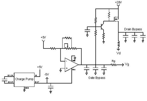
Figure 1: Common Bias Circuit for Large GaN HEMTs
Figure 1 shows a common bias circuit for large GaN HEMTs. A charge pump converts a positive voltage to a negative voltage to supply a bias setting op-amp. The components in the feedback loop of the op-amp set gate voltage and typically include a thermistor for temperature compensation and a potentiometer to set bias in production. When gate bias falls to the appropriate voltage range the PNP transistor pulls the PMOS FET gate low, turning it on, providing drain voltage to the RF device. The capacitor on the gate of the PNP delays turn-on of the drain voltage. In some applications controlled power-down is required and appropriate modifications to the bias circuit would need to be made to remove drain bias before gate bias. This circuit is currently being tested to verify component selection and operation, see the Nitronex GaN Essentials™ web content for final schematics and other information when testing is complete.
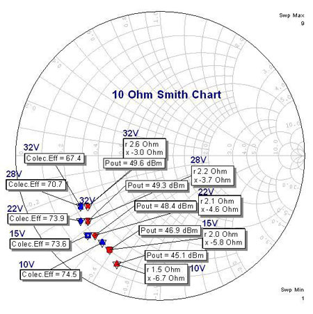
Figure 2: NPT25100 Peak Power and Efficiency Impedances Versus Drain Voltage
Drain Voltage is Your Friend:
Some GaN HEMTs maintain performance across a wide range of drain voltage. Nitronex GaN-on-Si HEMTs in particular are known for this characteristic. Figure 2 shows peak power and efficiency values and associated impedances across drain voltage for a 100W class device in a load-pull system. This is often a surprise to designers and can provide welcome flexibility from thermal management, power scaling, and power supply design perspectives.
Thermal Design:
High power density is a fundamental advantage of GaN. It leads to a shorter total FET width for a given power level, reducing total FET finger size and therefore reducing intrinsic device parasitics such as CGS and CDS. A typical 28V LDMOS FET has a power density in the range of about 0.7 W/mm, a typical 28V GaN HEMT has a power density of about 3.0 W/mm. The challenge with such high power density is getting the power from the junction to ambient surroundings effectively. A typical 120W peak power LDMOS FET has a thermal resistance in the range of 0.4 to 0.5°C/W. A typical 120W GaN HEMT devices has a thermal resistance of 1.8°C/W. The lower thermal resistance of LDMOS is due to both the inherent lower power density and multiple generations of device optimization. Future generations of GaN devices will close the gap substantially.
The critical point for an RF power amplifier designer is to check the thermal situation. What may have been 30% margin in the past could turn into 30% over budget in a new design. This could mean the total output power available from a GaN HEMT is limited by thermal design constraints, not inherent device capability. A common solution to thermal management is to run the GaN HEMT at reduced drain voltage to reduce power density on the die and lower peak junction temperatures. A 28V device specified for 100W may be a great choice for a 70W design at 22V. Figure 2 in the previous section shows performance across drain voltage for a 100W class GaN HEMT.
Robustness:
GaN HEMTs have been shown to survive output VSWR mismatches well compared to Si LDMOS and GaAs FETs. This can result in eliminating or simplifying protection circuitry and reduced field failure rates. Nitronex application note AN-004 shows the results of stress testing the NPTB00050 GaN HEMT. Devices were operated at 3dB gain compression and subjected to 10:1 and 20:1 output VSWR mismatches. No hard failures were observed and no significant change in gain, drain efficiency, and P3dB was observed The largest power droop was approximately 0.5dB in P3dB with a median change of 0.3dB. These tests were repeated and no additional shift was seen in the devices.
Conclusions:
GaN HEMTs offer improved efficiency over bandwidth, and improved robustness compared to existing Si and GaAs technologies. Some segments of the RF power amplifier market have already emerged for GaN HEMTs and they are quickly gaining ground in additional markets. This is leading to an increasing number of power amplifier designers leaning on GaN to meet their performance requirements. This column addresses some of the most common questions we hear from our customer base and can help ease the learning curve associated with using this new technology. Be sure to review the additional material in the GaN Essentials area of the Nitronex web site at www.nitronex.com.