
Thermal resistance is a measure of the amount by which the junction temperature rises for a given level of power dissipation in a transistor

Thermal resistance is important since it determines how much power a device and package combination can safely dissipate. Thermal resistance measurements normally require the measurement of a test diode and a thermally controlled environment. This article describes an approach that uses the gate or base of the device under test, rather than a separate test structure, and additionally can produce results without the need of a thermal chuck or oven. A single pulsed-measurement instrument and the device itself are used to generate different temperature points by setting different internal power dissipations. The approach is straightforward enough to be performed on a desktop computer. The test device can be a standard packaged part in the form that will be used in a circuit, including any heat-sinking arrangements.
The use of pulses, which are short compared to the thermal time constants involved, allows measurements to be made rapidly enough for the thermal equilibrium to remain undisturbed. The whole diode characteristic is obtained, which allows temperature to be deduced. This is in contrast to the traditional approach where a single point is measured, which requires careful calibration in temperature-controlled ovens or using other means of setting a constant thermal environment. The novelty of this method over the long accepted technique of using the temperature dependence of the forward diode voltage at a fixed current is that a complete diode characteristic is fitted. There are two significant advantages to this approach. First, the temperature can be deduced without the need of a pre-calibration procedure. Second, as part of the fitting process, the series resistance can be fitted, which eliminates the effects of parasitic resistance that may change with temperature. Examples of the technique, applied to both a FET and a bipolar device, are given.
Thermal Resistance
Thermal resistance is an important figure of merit for how well a transistor package and heat-sink combination is able to dissipate heat and thus to what power level the device may safely be run. Data sheets for commercial packaged parts give typical values for the general case. However, from the design engineer’s point of view, the thermal resistance of the device, as used in the designed circuit, is required. One option is to calculate an estimate, based on the data sheet value and data for the heat sink used, the thermal paste and so on. A more straightforward approach is to directly measure it, although such a measurement has previously required a means of measuring junction temperature, which in turn has required an additional sampling diode and a calibration procedure using some means of uniformly elevating the device’s temperature to a known value. This procedure is described in References 1 and 2, and runs to approximately thirty pages. The method described in this article requires only one temperature point, room temperature, thus avoiding the need for ovens or thermal chucks. Additionally, the forward conduction characteristics of the device itself are used to monitor the actual junction temperature.
Measurement Overview
The concept of thermal resistance assumes a linear relationship between the power dissipated in a device and its junction temperature. It is assumed that power dissipation has remained constant for long enough for thermal equilibrium to be attained. At zero power dissipation, the junction temperature should be room temperature (that is zero heating effect). An estimate of thermal resistance can, in theory, be made by measuring the junction temperature at just one elevated temperature point. In practice, better results will be obtained by making junction temperature measurements at several dissipated power levels and plotting a straight line through the results.
Thus, to measure the thermal resistance, the two variables to be measured are power dissipation and junction temperature. Power dissipation is simply obtained from the voltage drop across the device and the current through it. Junction temperature is more challenging and is discussed in the next section.
Measuring Junction Temperature
Since it is not possible to measure the junction temperature directly, an indirect approach must be used. The method used the effect the temperature has on the forward conduction characteristics of a diode. The test diode may be a separate device included in the test cell, close to the FET or bipolar under test, but it is also possible to use the gate or base as the test diode. In this article, it is assumed that there is no external test diode, so the base or gate of the device under test (DUT) must be used.
Though many large-signal models assume a diode-like behaviour for the gate of a FET or HEMT, or the base-emitter of a bipolar, in real devices, the behaviour is affected by the collector or drain terminal and may be far from being diode-like. For the method to work, the measurement of the diode current must be made with the collector of drain potential set to give a close approximation of the diode behaviour on the base or gate port. Measurements are thus best taken with zero, or close to zero voltage on the collector or drain port.
During the measurement, there will be almost no power dissipated in the device while the collector or drain is set to zero. The measurement must be performed fast enough so that there is no significant cooling of the junction during the measurement. In this work, a pulsed-measurement instrument (DiVA) was used to perform the measurements using repeated pulses, each of which was fast enough to prevent cooling from taking place. In brief, the measurement process is to set a range of different junction temperatures using different bias points for the device under test. At each bias point, the base or gate diode characteristics, with zero volt on the collector or drain, are measured using sufficiently fast pulses. The data is then analysed to obtain an estimate of the junction temperature for different power dissipations. The resultant points should lie on a straight line, the slope of which will give the thermal resistance.
Obtaining the junction temperature from measurement
The characateristics of a diode may be expressed in simple terms as

where
q = electron charge
k = Boltzmann’s constant
m = ideality factor
V = voltage across the diode (after accounting for any series resistance voltage drop)
T = temperature
For any fixed temperature, I0(T) is fixed.
Fitting the above equation to measured data at a fixed temperature (value of T) yields two parameters. One is I0(T) and the other is the product m·T. The first, I0(T), is a complicated function of temperature so the value of T is best obtained from the second parameter. The value of m is obtained by fitting the IV characteristics of the diode to the results with no junction heating (zero bias current) where T is known to be the room temperature. The same value of m can then be used to determine T at other temperatures, where there is power dissipation, giving rise to an elevated junction temperature.
Determining a Suitable Pulse Length
It is important to get the right pulse length for the measurement of the base or gate diode characteristics. If the pulse length is set too long, then there will be some cooling of the junction during the measurement itself, leading to erroneous results. If the value is set too short, then effects arising from cable capacitance or inductance may arise and trapped charges within the device itself may also affect the results.3
To determine a suitable pulse length for each sample device, the pulsed-measurement instrument was used to measure a transient current. The results of the transient measurement showed if there were rapid changes as well as slower thermal effects in the transient behaviour. The pulse length was set to be longer than the rapid changes arising from trapped charge movement, but still short enough to have no significant cooling during the pulse. Note that for completeness, it should be stated that some thermal effects can have very short time constants. This occurs when small devices are thermally isolated, perhaps by an isolation ring, so the volume to be heated is very small. But even in such cases, though the rise in temperature is rapid, the cooling may be a much slower process and so the method described in these notes may still be used to determine a relationship between dissipated power and junction temperature.
A Si Bipolar Example
To illustrate the method, a BF480 silicon NPN bipolar transistor was used. For this sample device, a pulse length of five microseconds was selected. The diode characteristics at zero volts were measured for the case of zero heating and at two higher levels of heating (power dissipation). Figure 1 shows the three measured characteristics along with the diode characteristic curves that were fitted to them. The parameters for the different cases are given in Table 1. For the zero power dissipation case, the temperature can be taken to be room temperature, which in this case was 28ºC or 301 K. From this, the value of m can be obtained

Using the value of m, the junction temperature, for the cases when there is power dissipated in the device, can be calculated. The results are shown in Table 2.

Fig. 1 Measured diode characteristics at three power dissipations for a BF480 (Si bipolar transistor).


Figure 2 shows a plot of the junction temperature rise versus power dissipation together with a straight-line fit. The slope of the line gives the thermal resistance between junction and case. The calculated value of thermal resistance is 467 K/W. The safe operating maximum power and junction temperature for a BF480 taken from the data sheet assume a thermal resistance of 714 K/W. Given that the data sheet must allow for the worst case of all samples plus a safety margin, the two values of thermal resistance are consistent with each other.
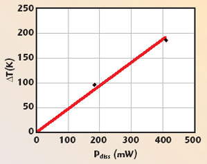
Fig. 2 Junction temperature rise versus power dissipation for the BT480 device.
A GaAs FET Example
As a second example, a GaAs FET was selected. The device is a CLY2 mounted in a brass jig. For this sample device, a pulse length of fifty microseconds was selected. (The CLY2 device is affected by trapped charges in deep levels so the pulse length must be long enough to enable such charges to redistribute.) As with the BF480 sample, the diode characteristics at zero volts were measured for the case of zero heating and at two higher levels of heating (power dissipation). Figure 3 shows the three measured characteristics along with the diode characteristic curves that were fitted to them. The parameters for the different cases are given in Table 3.

Fig. 3 Measured diode characteristics at three power dissipations for CLY2, a GaAs FET sample.

For the zero power dissipation case, the temperature can be taken to be room temperature, which in this case was 26°C or 299 K. From this, the value of m can be obtained

Using the value of m, the junction temperature for the cases when there is power dissipated in the device can be calculated. The results are shown in Table 4.

Figure 4 shows a plot of the junction temperature rise versus power dissipation together with a straight-line fit. The slope of the line gives the thermal resistance between junction and case. The calculated value of the thermal resistance is 28 K/W. The data sheet for the CLY2 states that the thermal resistance is less than 110 K/W. The measured thermal resistance is quite a bit lower than the given maximum value; this may be due in part to the jig acting as a heat sink.

Fig. 4 Junction temperature rise versus power dissipation for the CLY2.
Method Accuracy
To check the experimental results, measurements could be made at elevated temperature, using an oven rather than power dissipation within the device itself. Such measurements have not yet been made but the work is ongoing. The software used to fit the diode characteristics allows for a series resistance, which removes some of the uncertainty in the measurements. Taking the measurements at zero collector or drain voltage eliminates collector or drain current, which may introduce a voltage offset. As shown in Figure 5, the closeness of the fit to the diode characteristics gives some confidence that the base or gate is acting in a diode like manner under the measurement conditions.

Fig. 5 Comparison between calculated and measured characteristics of the BF480 device.
Conclusion
This article describes a means of measuring thermal resistance using a pulsed-measurement instrument without the need for a separate test diode or the use of a temperature-controlled oven for calibration. The results obtained are reasonable but further work is needed to make direct comparisons with results obtained using a thermally controlled oven to make an estimate of the accuracy of the method. The method used makes it easy to measure an overall thermal resistance even for complicated packaging and heat-sinking arrangements.
Acknowledgment
The author would like to acknowledge the extensive input to this work, through technical discussions, of Dr. Peter Ladbrooke.
References
1. “Integrated Circuits Thermal Measurement Method — Electrical Test Method (Single Semiconductor Device),” EIA/JEDEC Standard EIA/JESD51-1, December 1995.
2. J.W. Sofia, “Electrical Temperature Measurement Using Semiconductors,” Electronics Cooling, Vol. 3, No. 1, 1997, pp. 22–25.
3. P.H. Ladbrooke, “Pulsed I(V) Measurement of Semiconductor Devices with Applications,” Accent Optical Technologies 2004, ISDN 0-9762061-02.