
As mmWave systems advance toward higher frequencies, tighter integration and smaller form factors, a new reality has emerged: manufacturing precision is no longer just a metric — it is the defining factor in device performance. At frequencies in the tens or hundreds of gigahertz, electromagnetic behavior becomes highly sensitive to dimensional tolerances, internal surface quality and geometric complexity. Even minor deviations or surface roughness can cause insertion loss, signal distortion or severely degraded performance.
For decades, the RF industry has relied on conventional production methods such as CNC machining, electroforming and split-block assembly. However, as operating frequencies rise and internal geometries shrink into the sub-millimeter regime, these approaches are reaching their limits. They struggle to meet requirements for increasingly small, long or complex internal channels. Assembly challenges, limited design freedom and long lead times constrain innovation — precisely as next-generation aerospace, satellite communications, sensing and scientific applications demand more.
The Manufacturing Bottleneck
Serving customers across the electronics, testing, aerospace and medical sectors, Horizon Microtechnologies’ mission is to overcome design and manufacturing challenges by producing high performance 3D micro-parts. High-resolution photopolymer 3D printing offers exceptional geometric freedom but lacks the conductivity required for mmWave applications. Metal additive manufacturing, while conductive, is costly, insufficiently precise and produces rough surfaces. To bridge this gap, we required a workflow capable of producing complex internal features, enclosed channels and monolithic architectures with micron-level dimensional control, and of integrating advanced coating and metallization to achieve the required electrical performance.

Fig 1 S-parameters of a J-Band bandpass filter.
The Journey with Boston Micro Fabrication
Our search for a base manufacturing technology led to a strategic partnership with Boston Micro Fabrication (BMF). After early collaboration during product development, we integrated BMF’s micro-precision 3D printing platforms into our production lines. BMF’s Projection Micro Stereolithography (PµSL) technology addresses a critical “sweet spot” in precision, throughput and process stability unmatched in the current market.
In our experience, no other 3D printing approach balances this trade-off while maintaining comparable repeatability. Once a printing process is established, it delivers consistent, stable results. Over the past decade, additive manufacturing has evolved rapidly and these advancements have made it commercially viable for high-precision, miniature applications where every micron matters. Importantly, this enables production beyond prototyping. The industry’s “sweet spot” of 100 to 10,000 identical parts aligns well with micro-precision 3D printing, making it ideal for high performance RF components.
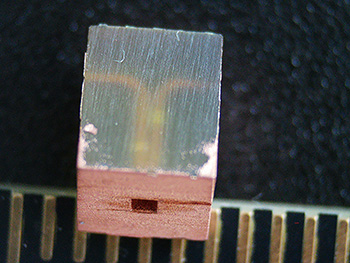
Fig 2 WR3 orthomode transducer made by 3D printing a polymer body and metalizing the inside surfaces.
Engineering the Impossible: Real-World Applications
By combining BMF’s microscale 3D printing with Horizon’s conformal metallization and application engineering, we have developed a workflow that enables the manufacture of mmWave components that were previously difficult — or impossible — to produce.
This approach is already supporting next-generation systems across four key areas:
1. High Performance RF Filters
Millimeter wave filters serve as spectral gates, isolating desired frequencies while suppressing unwanted signals.
Using BMF’s platform, we print intricate resonator cavities and coupling features as monolithic polymer structures with about 10-micron tolerances. We then apply a proprietary conformal metallization that coats smooth internal surfaces with a highly conductive layer that exceeds multiple skin depths (typically 2 to 10 µm). The Q-factor — a key performance metric — determines how sharply frequencies can be separated and directly affects data rates. It is highly sensitive to geometric precision, surface roughness and metallization quality. At higher frequencies, even small deviations significantly degrade performance. We have measured Q-factors exceeding 800 at 260 GHz on filters made using this approach, see Figure 1. This exceeds that of other 3D-printed filters at these frequencies and is comparable to results from advanced semiconductor-based fabrication methods such as silicon micromachining. Additional benefits include reduced weight and greater design flexibility.
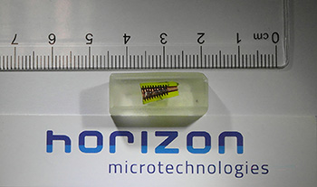
Fig 3 Inside a corrugated horn made by 3D printing and metallization.
2. Hollow Waveguide-Based Devices
Hollow waveguides are among the most challenging mmWave components to manufacture using conventional machining. They require precise cross-sections and smooth internal walls and typically rely on split-block construction, which introduces seams and alignment challenges. BMF’s micro-precision 3D printing technology enables the production of long, narrow and internally complex waveguide geometries as fully enclosed, monolithic structures. This eliminates seams, reducing leakage and assembly-induced losses.
After metallization, these waveguides exhibit electrically continuous internal walls with conductivity comparable to that of bulk copper. Figure 2 shows an example of a compact WR3 orthomode transducer that demonstrates low insertion loss, stable mode propagation, high separation efficiency and a reduced part count — with zero assembly tolerances.
3. Corrugated Horn Antennas
Corrugated horn antennas are widely used for beam shaping and high polarization purity. However, as frequencies increase, machining the required fine, periodic internal features becomes an absolute nightmare. Micro-precision 3D printing allows the entire horn (including corrugations, mode transitions and feed structures) to be produced as a single part with uniform depth and tight pitch control.
Post-production sectioning of WR5-range horns confirms that conformal metallization penetrates deeply into the corrugation grooves, preserving fine details and ensuring robust RF performance, see Figure 3. Compared with traditional approaches, these antennas are lighter and faster to produce, without the constraints of machining or electroforming.
4. Ceramic-Enabled Miniaturized RF Modules
As system integration increases, high-permittivity, low loss ceramics, such as alumina, are essential for miniaturizing components beyond the limits of air-filled waveguides. BMF’s platform enables the printing of ceramic green bodies with highly accurate geometries. After sintering, these parts reach full density with predictable shrinkage, preserving the original precision.
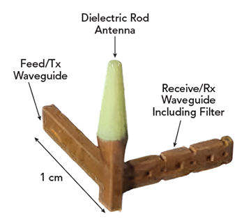
Fig 4 Ceramic-loaded metalized waveguide plus antenna assembly consisting of a dielectric rod antenna, a waveguide filter and a feed waveguide.
Full or selective metallization then produces fully functional dielectric-loaded components. Figure 4 shows a 50 GHz module that integrates a waveguide feed, junction, rod antenna and filter into a single alumina body. This achieves roughly a three-fold reduction in each dimension compared with equivalent air-filled systems while maintaining stellar electromagnetic performance.
The Future is Monolithic and Scalable
As mmWave technologies continue to expand across telecommunications, aerospace and medical sectors, manufacturing capabilities dictate what is functionally possible. Higher frequencies demand tighter tolerances and smoother internal surfaces than legacy methods can reliably achieve. The integration of micro-precision 3D printing with advanced functional coatings marks a paradigm shift. The industry is moving away from multi-part assemblies toward monolithic, highly integrated component architectures. These coated parts also undergo rigorous testing under real-world operational stresses.
By eliminating assembly complexity and expanding design freedom, precision additive manufacturing is no longer just a prototyping tool but a production-ready pathway to lighter components, faster innovation cycles and entirely new RF architectures.
The future of mmWave manufacturing is no longer about accepting the limits of traditional machining. It is about engineering at the microscale with absolute precision, ensuring every component performs flawlessly under the most demanding conditions.