
Advanced packaging has become the scaling vector for computing power, and it is increasingly the scaling vector for RF systems, too. The same forces that reshaped compute, such as chiplets, 2.5D/3D stacking, denser redistribution layers and new production formats, are now reshaping RF front ends as they expand in band count, antenna count and integration level. Packaging is no longer just an enclosure: at mmWave and sub-THz bands, it becomes part of the electromagnetic design, the thermal architecture and the cost structure.
That shift is widening the materials palette. One of the most consequential additions is glass, as shown in Figure 1. Historically linked to displays and optics, glass is now emerging in advanced packaging through multiple entry points, and that multi-entry nature is precisely what makes it strategically interesting. Glass is arriving at different “levels” of packaging: carrier, interposer, substrate and even board-level, each solving different bottlenecks and each reinforcing the others through shared equipment, process know-how and supply chain investments.
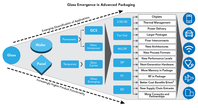
Figure 1 Glass emergence in advanced packaging. Source: Glass Materials for Packaging 2025 report, Yole Group.
In parallel, RF system requirements are converging with the compute packaging roadmap. RF wants low losses, stable geometry, dense vertical interconnects for shielding and waveguide structures and compact antenna-feeding networks. Compute wants dimensional stability for ultra-fine routing and large body sizes, as well as scalable manufacturing formats. Glass sits at that intersection.
Glass fits both “compute scaling” and “frequency scaling.” At the material level, glass offers a mix that is unusual in one substrate family: a wide dielectric constant range (3.7 to 21), CTE tunability (3 to 12 ppm/K) and very smooth surfaces (<10 nm roughness), with zero moisture absorption listed in comparative packaging tables. These features become increasingly valuable as frequencies rise and line widths shrink. Glass also aligns with the manufacturing direction of travel: it can be produced and processed in large-panel formats, positioning it between expensive silicon interposers and cost-sensitive organic laminates for mmWave applications.
For RF specifically, the physics drivers get harsher above ~100 GHz, where the conductor roughness penalties grow, discontinuities matter more and parasitics that were tolerable at 6 to 28 GHz become dominant error terms. Glass-based approaches are being actively discussed for W-Band, D-Band and even G-Band packaging. This is why packaging choices increasingly translate into system cost and performance, not just manufacturability.
For the system architecture, the direction is clear: tighter co-location of antennas, RFICs/MMICs, mixed-signal and compute. The “antenna-to-AI” concept popularized for 6G is essentially a packaging roadmap that compactly integrates MMICs, passives and compute to collapse latency, loss and form factor across the RF-to-data path. Glass becomes relevant because it can serve as both an RF-friendly substrate and a scalable integration medium.
MULTI-ENTRY ADOPTION OF GLASS IN PACKAGING
The multiple entry points allow glass to be treated not as a single product, but as a platform with four entry points and practical roles, including glass carriers, glass interposers, glass-core substrates and glass at the board level, as shown in Figure 2. Each role has its own adoption curve, RF relevance and bottlenecks.
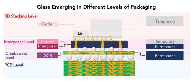
Figure 2 Glass emerging in different packaging levels. Source: Glass Materials in Semiconductor Manufacturing 2025 report, Yole Group.
Glass is already widely used, often “quietly,” as a carrier in advanced packaging flows, particularly when thin wafers or fragile stacks require stiffness and planarity. This includes fan-out processes, thin-die handling and some 3D stacking steps. The carrier role is one reason why glass’s ecosystem is maturing faster than usual for a new material; CapEx investments can be justified even before glass becomes the permanent substrate.
Glass Interposers
A glass interposer is the closest conceptual analog to a silicon interposer. A thin dielectric plate with dense through-glass vias (TGVs) and fine redistribution layers (RDL), used as an intermediate routing and interconnect layer between dies/chiplets and the package substrate.
Why does this matter in compute packaging? Computing is pushing 2.5D/3D into a regime where interposer size and routing density can dominate cost and yield. Silicon interposers deliver superb density and alignment, but cost and wafer-size constraints become painful as body sizes grow. Organic and molded interposers offer cost advantages, but face limitations in geometry control, moisture behavior and ultra-fine scaling. Glass interposers occupy the “middle ground.” They aim for the precision of silicon-like routing without silicon RF’s leakage behavior and with an eventual path to panel-scale throughput. Glass keeps resurfacing due to the equipment ecosystem and its adaptability to panel formats adapted from the flat panel display industry.
RF receives a second benefit. Glass interposers are not just dense routing planes, they can be engineered as electromagnetic structures, including as via fences and ground cages for isolation between RF channels and between RF/digital regions, substrate integrated waveguides (SIW) and waveguide-like cavities (especially attractive at D-Band+), antenna feed networks with tighter phase and amplitude control and embedded passive integration (filters, couplers, transitions) that reduces board-level loss and assembly complexity.
The telecommunications industry can commercialize it faster “in RF” because the value proposition (loss, integration and size) is so immediate for mmWave front ends and backhaul modules. In practice, RF modules increasingly need low loss routing to arrays, tight tolerances to maintain beam patterns and compact transitions that do not destroy match and efficiency. Glass interposers directly target these requirements, as demonstrated in Figure 3.
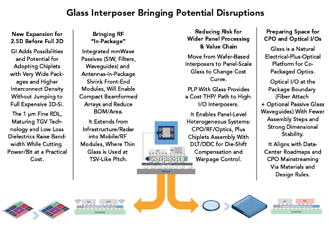
Figure 3 Glass interposers bringing potential disruptions. Source: Glass Materials in Semiconductor Manufacturing 2025 report, Yole Group.
GLASS-CORE SUBSTRATES
A glass-core substrate places glass in the role traditionally played by an organic core, the structural backbone of the IC substrate. Built-up dielectric layers and copper routing are then formed on one or both sides, often symmetrically, to manage warpage.
Data center servers and AI accelerators are reaching the limitations of organic IC substrates in terms of larger body sizes, higher layer counts and finer routing. These demands amplify the problems of warpage and dimensional drift. Glass, with a wide CTE spectrum and high stiffness, is positioned as a way to improve dimensional stability, reduce warpage and enable higher routing density. Intel’s September 2023 announcement on developing glass-core substrates is a notable inflection point in the substrate-level glass industry. That announcement matters not only because of the technology, but because it signals ecosystem-changing dynamics: raw glass suppliers, chemical suppliers, laser equipment suppliers, new glass-based business models, inspection and assembly qualification. Since the announcement, the number of companies involved has exploded from research and development projects to the formation of consortia and the building up of pilot lines.
For RF, a glass-core substrate is not always about the last micron of line/space. It is often about geometry stability for arrays, in which phase consistency and calibration across temperature, lower dielectric loss foundations for mmWave feed networks and filters, better isolation structures enabled by vertical vias and stable build-up alignment and also the integration of RF and digital in a single substrate when radios incorporate significant local compute (beamforming, MIMO, AI-assisted calibration).
Interposers can improve performance quickly, but substrates are where volume economics live. Glass-core substrate (GCS) adoption is therefore less about “can it be built?” and more about “can it be built at the yield, cost and reliability required for high volume platforms?”
THE REAL SCALING PRIMITIVE: TGV KNOW-HOW
If glass interposers or GCS are the architecture, TGV is the primitive. In Si interposers, TSV technology is mature. In glass, the process window is different (drilling and etching, metallization adhesion, void-free fill and substrate edge warp and reliability error crack management). The industry target is clear: shrink via diameters, improve placement accuracy and scale throughput.
RF packaging uses glass in several additional ways that can become mainstream even if glass interposers or GCS take longer to scale.
Antenna-in-Package Arrays and Feed Networks
As arrays grow (more elements, tighter spacing), the feed network becomes a dominant source of loss and phase error. Glass offers a stable, low loss routing plane with the potential for fine pitch and tight tolerances, useful for beamforming modules (phased arrays for 5G/6G access, backhaul and radar) and also compact front ends where antenna, filters and transitions are co-located.
Integrated mmWave Passives
At D-Band and beyond, integrated waveguide structures become attractive. Glass supports dense vias and can be combined with cavities, including air features in some approaches, enabling compact low loss passive functions. The SIW, filters and waveguides are part of the “RF in-package” value proposition, shrinking discrete front ends into packaging-level integration.
Embedded Die and Cavity-Based RF Modules
Embedding RF die inside glass cavities shortens vertical RF paths and reduces transition discontinuities, often the hidden limiter at mmWave/sub-THz. This mirrors compute packaging’s move toward embedding and stacking (high bandwidth memory, logic-on-logic), but with different design goals: impedance continuity, isolation and minimizing radiation and leakage.
Board-Level and System-Level Explorations
A small but important set of efforts explores glass-like materials or glass cores at larger scales (low loss backplanes, stable high speed routing or hybrid electrical/optical interfaces). Even when these are at an early stage, they reinforce the same ecosystem: drilling, metallization, inspection and panel handling.
GLASS: WHAT NEXT?
Glass is no longer just a low loss dielectric. It is increasingly being engineered as a multi-role packaging platform: as a carrier enabling thin-wafer and panel processes, as a glass interposer enabling dense vertical interconnect and fine RDL for 2.5D/3D chiplets and mmWave passives and as glass-core substrates aiming to deliver the dimensional stability and routing density needed for the next generation of large, high-end packages. The multi-entry view helps explain why momentum is accelerating: each role can mature in parallel, reinforcing ecosystem investment and pulling glass from specialty use into scalable production pathways.
For RF, the timing is particularly compelling. As front ends move from sub-6 GHz into mmWave and onward to sub-THz, advanced packaging becomes an RF component, and the substrate must deliver low dielectric loss, smooth conductors/interfaces and tight dimensional stability for fine routing and scalable interconnect density. Glass’s property envelope, dielectric constant range, tunable CTE and ultra-smooth surfaces map directly onto these requirements, and its panel compatibility aligns with the industry’s push to new manufacturing formats.
The remaining question is not whether glass works, but how fast the ecosystem can convert process maturity, especially around TGV formation/fill, panel handling, warpage control and RF/thermal co-design, into repeatable, cost-competitive, high volume manufacturing. That ramp will likely occur unevenly: RF infrastructure and specialty mmWave modules may adopt first where performance value is immediate, while AI/HPC and substrate-level adoption will accelerate as supply chains and panel yields reach the scale demanded by mainstream compute platforms.