
The demand for greater communication bandwidth on a global scale is growing. As a result, next-generation satellites must deliver higher data throughput for digital payloads. Among in-orbit configurations, edge computing and other advanced needs, current FPGAs and ASICs call for greater power requirements. The shift to digital payloads requires engineers to reassess key design parameters, such as material needs, operational factors and radiation robustness, to ensure reliable performance in their space power systems.
For generations, silicon (Si) has been the industry’s material of choice in power applications; however, in recent years, GaN has shown promise, offering a multitude of advantages in applications where reaching high switching speeds and efficiency are equally as important as minimizing the size and weight of a power system. GaN use in space applications is expanding due to the benefits of using a wider bandgap semiconductor to optimize operations and its performance as a radiation-hardened (rad-hard) high electron mobility transistor (HEMT). Infineon IR HiRel manufactures rad-hard GaN transistors with JANS qualification.
TECHNOLOGICAL ARCHITECTURE OF GAN
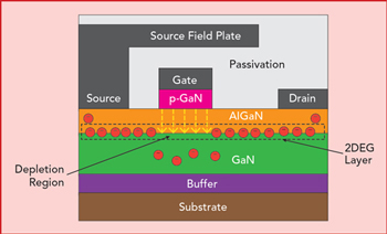
Figure 1 Cross-sectional structure of GaN HEMT.
GaN holds a bandgap energy of 3.4 eV. In comparison, legacy technology, such as Si, has a bandgap energy of 1.1 eV. The material properties of wide bandgap semiconductors such as GaN make the technology suitable for power transistors. Figure 1 illustrates the general design of Infineon IR HiRel’s lateral GaN HEMT, IG1NT052N10R. Electrons move from the source to the drain through a 2-dimensional electron gas (2DEG) layer formed at the AlGaN and GaN epi heterojunction layer. This is a result of a piezoelectric effect that occurs at the interface between the two layers. A layer of positively doped GaN, p-GaN, is integrated between the gate and AlGaN layer to produce a depletion region. The inclusion of a p-GaN layer allows the transistor to have a positive threshold voltage and perform as an enhancement-mode device. This structure plays a role in the benefits of GaN as a power transistor technology. The source field plate reduces the peak electric fields found on the gate. The 2DEG layer allows high mobility of electrons with minimal drain-source resistance (RDS(on)), a key parameter to account for in power transistors. Low Vth, such as 1.5 V for IG1NT052N10R, results in higher switching speeds. The structure of a lateral GaN HEMT also lacks a gate oxide that is typically observed in Si MOSFETs. As a result, GaN has a slight robustness to radiation inherent to its design. However, rad-hard by design is still applicable to GaN, as some parameters need to be mitigated under radiation.
RADIATION AND POWER PERFORMANCE
There is some inherent robustness to GaN under various radiation effects due to the absence of a gate oxide. GaN faces no trapped charge nor VGS(th) shift under total ionizing dose (TID) radiation and does not suffer from single event gate rupture (SEGR) under single event effect (SEE). Even though GaN has inherent radiation resistance, there is still an advantage to choosing rad-hard solutions over commercial-off-the-shelf (COTS) parts for space applications. Figure 2 demonstrates the importance of creating a GaN transistor that is rad-hard by design. Comparing a COTS-graded GaN to a rad-hard GaN, it is observable that the COTS device significantly drifts while the rad-hard GaN remains relatively stable over the entire duration. Radiation hardened by design will often ensure the reliability required in extreme environment applications. Figure 3 highlights the radiation robustness of GaN under SEE for three different lots tested up to Au. In addition to how the GaN device under testing does not require derating when subjected to LET of 70 MeV*cm2/mg (the LET Si equivalent to 86.5 MeV*cm2/mg), the electrical operation of the device is up to standard with the industry’s leading rad-hard transistor standards. To make sure the device is suitable for power architectures in space systems, Infineon IR HiRel created a new package specifically for GaN, called the PowIR-SMD.
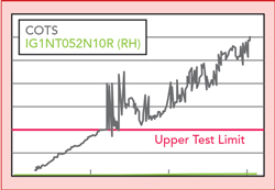
Figure 2 SEE flux radiation versus
drain-source leakage current.
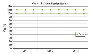
Figure 3 SEE SOA for IFX IR HiRel 100 V RH GaN HEMT.
Infineon IR HiRel developed a new surface-mount package to ensure reliability and robust operations for its rad-hard GaN device. Minimizing parasitic inductance is imperative in system design because GaN is a fast-switching technology. Infineon IR HiRel developed the PowIR-SMD to be a bond wire-free SMD package that has an inductance value of 0.1 nH. Additionally, this package allows a Kelvin-source connection to decouple the gate drive from the power stage, lowering the common-source inductance of the device.
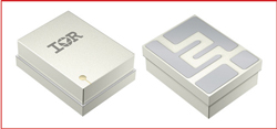
Figure 4 3D representation of PowIRSMD.
Another factor to address is the CTE mismatch between the packaged device and the PCB. Occasionally, ceramics such as alumina are developed into hermetic packaging to address such mismatches. This is seen with Si MOSFETs, where the devices are large enough to dissipate the heat generated. The high density of GaN allows the technology to perform efficiently within a smaller form factor compared to Si MOSFETs. Consequently, packages dedicated to GaN would benefit from developing a package consisting of aluminum nitride, AlN. The higher thermal conductivity of AlN compared to alumina, 150 W/m*K versus 12 W/m*K, respectively, allows the device to dissipate heat more effectively. The size of GaN, in this case, is small enough to mitigate the thermal cycling mechanical stress concern that is considered when using AlN. The inclusion of AlN holds an additional benefit as it lessens the accumulation of free charges from environmental radiation, preventing system damage and contributing to inherent radiation robustness. Figure 4 illustrates a 3D representation of a hermetic package, PowIR-SMD, a surface-mount packaging dedicated to addressing GaN usage in space.
CONCLUSION
The increasing demand for higher processing power in satellites has led to a growing need for advanced technologies that can handle complex tasks such as artificial intelligence, in-orbit reconfiguration and more. High-power FPGAs and ASICs are being driven to their limits, and as a result, improved efficiency and reduction in size and weight are critical factors to consider in satellite design.
Infineon IR HiRel’s rad-hard GaN HEMT brings radiation performance and electrical robustness to the high-reliability market. The 100 V rad-hard GaN HEMT, now available under MIL-PRF-19500 JANS qualification, has been designed to optimize performance in power systems.
Infineon Technologies
IR HiRel
Andover, Mass.