

While the terms “power divider” and “power splitter” are often used interchangeably, there is a fundamental difference in their designs and intended applications. Power dividers (2-way) typically utilize a three-resistor configuration and are used for dividing a single input signal into multiple output signals for applications such as signal distribution. Power splitters, often employing a two-resistor configuration, are primarily used for leveling and ratio measurements. Both power dividers and power splitters can function as power combiners.
POWER DIVIDERS

Figure 1 1:2 three-resistor power divider schematic.

Figure 2 1:4 power divider schematic a) in a star pattern and b) as concatenated 1:2 power dividers.
A three-resistor RF power divider, shown in Figure 1, is a passive circuit that produces a 1:2 split of an incoming RF signal into two output signals. The design typically uses three resistors having a value of 16.6 Ω, often in a star or tee configuration, to divide the power while maintaining a consistent impedance match and signal integrity across a wide frequency range, assuming all ports are terminated in 50 Ω. These dividers are known for their simplicity and wide bandwidth, but they also introduce insertion loss due to the resistive nature of the circuit. Assuming all outputs are terminated into 50 Ω, the RF power divider presents a 50 Ω load to a signal source connected at Port 1 (input). In this case, the device transmits one quarter of the input power, or -6 dB, to Port 2 and Port 3. 3 dB of the loss is generated from the power dividing, and 3 dB of the loss is generated in the resistors.
These devices can be manufactured in several ways, including a series of surface-mount thin film or thick film resistors on a printed circuit board or a series of thin film resistors made of tantalum nitride (TaN) or nichrome (NiCr) on a ceramic substrate. TaN resistors are very stable and reliable after they are passivated at high temperatures, whereas NiCr resistors are used in specialty applications where a low temperature coefficient of resistance (TCR) is required.2 The power handling capability of the circuit is mainly based on the size of the resistors and the ability of the device to either control or disperse the heat generated from the resistive loss.
Power dividers are usually specified by the power handling and bandwidth of the circuit and the amplitude and phase balance of the two output ports relative to the input port. Since the circuit is a resistive, passive design, it functions from DC to the maximum cutoff frequency of the design. There are currently offerings on the market with bandwidths specified from DC to greater than 110 GHz.
Power dividers can be designed to have more than two outputs by concatenating multiple 1:2 power dividers or by using a greater number of resistors sharing a common node. Figure 2 shows two examples of manufacturing a 1:4 power divider. Figure 2a incorporates five 30 Ω resistors in a star pattern. This methodology has some drawbacks in dividing the power of the input signals equally among the remaining four ports due to the physical symmetry of the design. At high frequencies, more energy enters the ports opposite the input than enters the adjacent ports.
A more common implementation is to use three 1:2 power dividers, shown in Figure 1, resulting in the schematic shown in Figure 2b. This topology ensures equal power division, each -12 dB down from the input signal, and an identical group delay across the four outputs. The main drawback to the topology shown in Figure 2b is that the power divider has a dedicated input port, and the isolation between each of the output ports is not identical.
The final power divider for discussion is one that creates an unequal power division between the two outputs. Figure 3 shows a topology where all the ports are matched to 50 Ω, but the power delivered to Port 2 and Port 3 is unequal. This component is more commonly referred to as a resistive coupler or an impedance-matched pick-off tee. A common (unequal) divider ratio would select the four resistors to supply -4 dB to Port 2 while supplying -10 dB to Port 3 (both relative to Port 1), while keeping all three ports matched to 50 Ω.

Figure 3 Unequal power divider schematic.
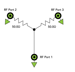
Figure 4 1:2 two-resistor power splitter.
POWER SPLITTERS
A two-resistor RF power splitter, shown in Figure 4, is a passive circuit that produces a 1:2 split of an incoming RF signal into two output signals. This design typically utilizes two resistors, each having a value of 50 Ω. A power splitter is a simple and common method to split power in RF circuits, particularly in applications like gain measurements and leveling loops.
The input impedance at Port 1 is matched to 50 Ω when the outputs, Port 2 and Port 3, are terminated in 50 Ω. In contrast, the outputs of the resistive power splitter look like 83.3 Ω when all ports are terminated to 50 Ω.
The unique feature of a power splitter is best defined when the port impedance on both Port 2 and Port 3 is not 50 Ω and/or unequal. In this case, the power splitter delivers equal incident power to both loads irrespective of the load imbalance. Since equal incident power is constant regardless of load impedance imbalances, the two-resistor power splitter is used where the ratio of output power to a reference signal is needed. To understand this phenomenon further, one must review 3-port network theory and investigate the scattering parameters (S-parameters) of both the power divider and the power splitter.
3-PORT NETWORK THEORY

Figure 5 Three-port device flow diagram.
To better understand the function of a power divider versus a power splitter, it is helpful to review the S-parameters of 3-port RF devices. A 3-port network can be visualized as shown in Figure 5.
Referring to Figure 5, each port is represented in terms of inward-going (incident) voltage wave “an” and outward-going (reflected) voltage wave “bn.” The subscript “n” represents the port number associated with the wave. S-parameters can be used to represent voltage transfer functions within and across ports. By definition, each port that is not being actively stimulated with incident energy is assumed to be terminated with a 50 Ω load. For example, S11 is the ratio of the reflected “b” wave at Port 1 (b1) to the incident “a” wave at Port 1 (a1) with no signal applied at the other two ports.
Similarly, S21 is the ratio of the outward-going “b” wave at Port 2 (b2) to the incident “a” wave at Port 1 (a1) with no signal applied at the other two ports.
A full linear matrix shown in Equation 3 can be used to describe the incident and reflected wave relations of a 3-port device as follows.
S-PARAMETERS OF POWER DIVIDERS AND SPLITTERS
The fundamental differences between three-resistor power dividers and two-resistor power563 splitters are well understood and documented in literature.1 The work by B. Smith presents the differences between the two components and derives the scattering parameters of both devices.1 These results are best summarized in Table 1.

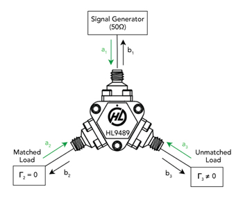
Figure 6 Power splitter example with an unmatched load.
The three-resistor power divider has an impedance match, resulting in no reflections on all ports (S11=S22=S33=0) and 6 dB of isolation between output ports (S23=S32=0.5). In contrast, the power splitter has 12 dB return loss on the output ports (S22=S33=0.25) and 12 dB of isolation between output ports (S23=S32=0.25). This gives the power splitter a distinct advantage when driving imbalanced loads. If energy is reflected from an unmatched load and arrives back at the output of the power splitter, one quarter of that energy is re-reflected, and one quarter is transmitted to the opposite output. “This maintains an equal power output from the two ports”.1 This scenario is illustrated in Figure 6.
The parameters in Equations 3 and 4 become apparent when inspecting the forward and reflected waves.
Using the data in Table 1, one can now see the advantages of a power splitter by looking at the expressions in Equations 6 and 7. The equations show that the energy reflected from the unmatched load on Port 3 is equally re-reflected to both Port 2 and Port 3, keeping the ratio of the two outputs at a constant.
POWER SPLITTER – APPLICATION
One application for a power splitter is a ratio measurement, as shown in Figure 7. This setup will provide a ratio of the transmitted signal through the device under test (DUT) relative to the detected signal on the second power splitter output. This measurement will result in the gain of the DUT.
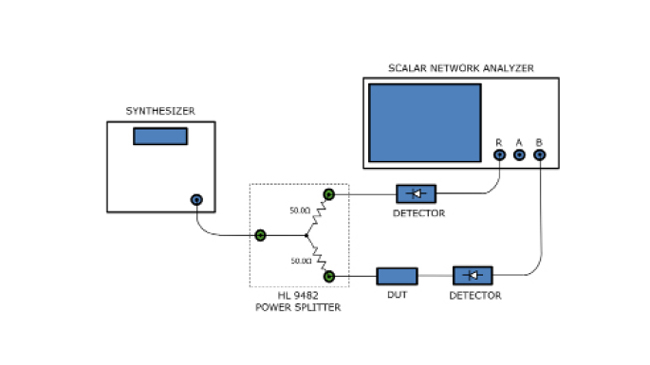
Figure 7 Ratio DUT transmission measurement using a power splitter.
The previous S-parameter calculations demonstrate that both outputs of the power splitter are identical (S21 = S31) and that the reflections from the DUT are equally split to both outputs of the device. With this knowledge, it is assured that only the gain of the DUT is being measured, regardless of the impedance seen by the output of the power splitter that is driving the DUT.
POWER DIVIDER - APPLICATION
A standard application for a power divider, shown in Figure 8, is to use it for clock signal distribution. In this application, the power divider is being driven with a clock signal generated by an RF synthesizer. Once the clock signal is divided into two identical signals, one signal can be used to drive the DUT, and the other can be used to drive the phase reference module of the equivalent-time sampling scope.

Figure 8 Power divider used as a clock fanout.
In any application where a clock signal needs to be duplicated, a power divider will create two or more in-phase versions of the clock source.
CONCLUSION
Power dividers and power splitters are both devices that divide/split an input signal into multiple output signals, but they differ in their design and intended use. Three-resistor power dividers are designed to distribute power evenly among multiple output ports, while two-resistor power splitters can be designed for various power division ratios and applications.
This article is intended as an introduction to the differences between power dividers and power splitters by presenting the S-parameters that differentiate them from one another. Specific application examples have been provided for each device to help further the understanding of the noted differences.
References
- B. Smith, “Choosing the Right Power Splitter: Two-Resistor or Three-Resistor.” Power Splitter vs. Divider, www.dinfo.unifi.it, n.d.
- “Design Guidelines,” UltraSource, [Online]. Available: https://www.yourthinfilmsource.com/design-guidelines/.