

Following the completion of this step, it is possible to move to the next setup, a near-field socket (Figure 4b). The small physical size of the socket allows for multi-site testing in production while still providing OTA parametric measurement results. At this stage, the test engineer can correlate the measured results using this setup with the previous far-field setup results to define the appropriate correlation/correction factors and pass/fail thresholds. Note that the test program, PCB test fixture and measurement instruments are the same as for the far-field setup, significantly reducing the test engineer’s development effort.
The final setup (Figure 4c) is the complete HVM multi-site production test cell, including the robotic handler where high volumes of AiP DUTs can be tested and automatically binned into good and failed devices.
RADIATING NEAR-FIELD OTA HVM TESTING
As previously mentioned, using a near-field OTA socket provides OTA parametric measurements while allowing multi-site integration on a standard commercial ATE test cell due to the small physical size of the socket compared to a far-field measurement setup.

Figure 5 Far-field and near-field OTA sockets.
Figure 5 details the manual far-field and near-field OTA sockets. The far-field socket comprises a traditional electrical socket base (e.g., spring pin or elastomer) and a lid to push the DUT into the socket for reliable electrical contact. The challenge in OTA testing is that the socket body matters, and the lid material directly impacts the DUT antenna array performance.1
Special care must be taken in the choice of socket body materials and the socket design to minimize the impact on the DUT antenna array performance. This is not trivial since one needs to optimize between the electromagnetic requirements that prioritize having no material close to the antenna array and the mechanical requirements that mandate a lid on the socket, as well as some self-alignment features for reliable insertion of the DUT in the socket.4
Any material close to the DUT antenna array must have a very low dielectric constant, which often means low mechanical strength. For example, a typical lid material is Rohacell HF75 with a dielectric constant of 1.09 but a Young’s modulus of 92 MPa. A typical socket material is PEEK because of its mechanical strength (35000 MPa Young’s modulus), but it has a dielectric constant of 3.2. This means OTA sockets are usually a hybrid of different materials, as shown in Figure 5.
Another critical part of the near-field socket is the measurement antenna, as shown in Figure 5. The measurement antenna aperture in this example is located 3 cm from the DUT antenna array. The measurement antenna not only has to cover the application frequency range (e.g., 24 to 56 GHz for 5G frequency range 2) and polarization (such as dual linear polarization), but also must have a low profile due to mechanical requirements for later integration in a multi-site production handler. Because of these requirements, the socket antenna design is unique compared to traditional antenna designs.5
Figure 6 illustrates two significant challenges associated with a near-field OTA socket testing approach. The first (Figure 6a), is that the measurement antenna will not be able to measure all the antenna elements equally, as in the case of far-field OTA testing. This is where golden device calibration is critical for properly correlating the measured results for each antenna element. The second challenge is that the measurement antenna is now so close to the AiP DUT antenna array that it might impact the DUT AiP antenna elements (antenna detuning) and result in a standing-wave effect. This is shown in Figure 6b, where two patch antennas are simulated with varying distances between them. This challenge is addressed by correctly choosing the distance between the measurement antenna and the DUT antenna array in the socket. The objective is to avoid the test frequencies used in the test plan being located at the resonant standing wave frequencies. Advantest has developed an automated procedure to determine the optimized distance given a set of test frequencies.6 Note that, if properly designed, the absorber structure inside the socket, shown in Figure 5, can significantly help to mitigate this problem.1
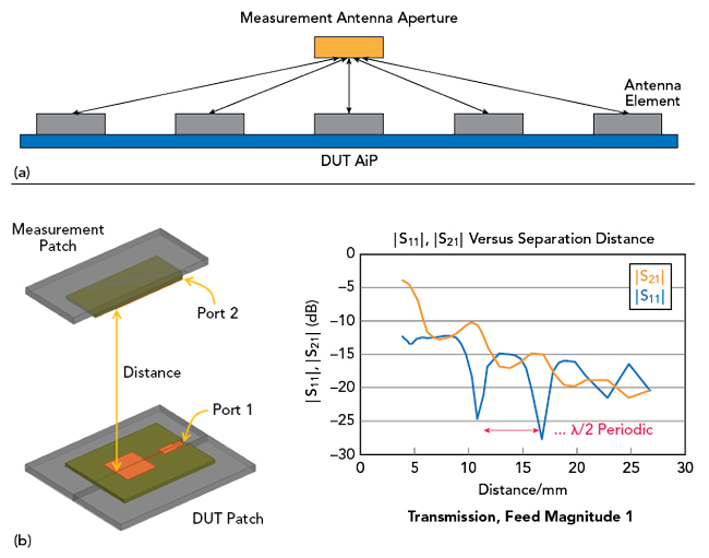
Figure 6 Near-field measurement variation due to (a) the antenna element position and (b) the standing wave effect between the socket measurement antenna and the AiP antenna array.
HANDLER INTEGRATION
To enable OTA testing in HVM, it is necessary to integrate the OTA socket, including the measurement antenna, into a standard commercial handler. There are two potential options (see Figure 7). One approach uses a dead-bug configuration, as shown in Figure 7a.7 This approach can initially be appealing because it avoids the challenge of integrating the measurement antenna into the handler arm, making it a part of the DUT test fixture instead. Unfortunately, it significantly increases the complexity of the DUT test fixture assembly and requires a more electrically complex socket.

Figure 7 Diagram of handler integrations for OTA testing: (a) dead-bug and (b) live-bug.

Figure 8 Hontech handler with the Advantest OTA change kit.
The second option is to use the traditional live-bug approach, as shown in Figure 7b, where the handler arm picks the DUT and pushes it into the DUT socket. In an OTA setup, because the antenna is integrated on the handler arm, it requires an mmWave blind-mate interconnect that can handle many docking cycles.8,9
Figure 8 provides an example of such an implementation for an 8-site OTA change kit in a Hontech HT-9046LS handler. One arm is used to pick and place the DUTs on the sockets and the other arm is used for the OTA testing and contains the measurement antenna and blind mating waveguide interconnects.
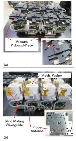
Figure 9 Handler integration showing (a) pick-and-place handler arm and (b) handler arm with socket lids and probe antennas.
Figure 9 shows the handler OTA change kit attached to each handler arm in more detail. In this picture, the absorber element is not shown, but it is critical not only to address the unwanted effects inside the small socket space but also to improve isolation between the adjacent sites, as shown in Figure 10.1
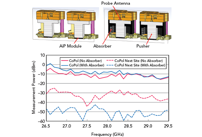
Figure 10 Simulation of the crosstalk between two adjacent sites with and without the RF absorber element.
Another critical point in the handler integration is DUT temperature control — not only to control the integrated die temperature during testing, which can impact the measured performance, but also, in specific applications, to test the DUT at cold and hot temperatures. This can be done by directly controlling the temperature of each DUT or by controlling the temperature in the handler chamber.
Another OTA challenge for handler integration is the testing of L-shaped AiP modules.10 These modules can also be tested with a standard commercial handler.11 Although this article has not shown measurement results, see Reference 12, a custom-designed AiP demo vehicle is used to demonstrate some possible OTA measurements and correlation results.12
Conclusion
The presented HVM OTA test solution from Advantest uses the established testing infrastructure at the back end of the semiconductor manufacturing industry to test mmWave AiP modules with a high failure coverage by using OTA parametric measurements. With the use of multi-site configurations on standard ATE test cells, the solution delivers a lower CoT.
Acknowledgments
The author would like to thank Natsuki Shiota, Aritomo Kikuchi, Hiroyuki Mineo, Hiromitsu Takasu, Frank Goh, Sui-Xia Yang, Roger Nettles, Kato Yasuyuki, Atsushi Nakadate and Shinji Fujita from Advantest and Prof. Jan Hesselbarth from Stuttgart University for their contributions to this project.
References
- J. Moreira, A. Papanikolaou and J. Hesselbarth, “High-volume OTA Production Testing of Millimeter-wave Antenna-in-package Modules,” IEEE Open Journal of Instrumentation and Measurement, Vol. 4, 2025.
- “Advantest Leading Parametric OTA Solution for 5G AiP Modules,” https://youtu.be/9xbYj4-DOHE.
- P. Cockburn, “A 55GHz Octal-site Probe Card for 5G mmWave Devices,” Chip Scale Review, July/August 2022.
- J. Moreira et al., “Design of a DUT Socket for OTA Testing with Automated Test Equipment,” to be published at the International Symposium on Antennas and Propagation (ISAP), 2025.
- J. Moreira et al., “Dual-Polarized Quad-Ridged Waveguide Antenna for OTA Near-Field ATE Socket in 5G-FR2 Band,” 28th IEEE Workshop on Signal and Power Integrity, 2024.
- J. Moreira, Patent Application WO2024260540A1.
- B. C. Wadell, “Results of a Handler-based Solution for 60 GHz AiP DUT,” SEMICON West Test Vision Symposium, 2022.
- J. Moreira, S. Churkin and J. Hesselbarth, “A Double-ridged Design for 5G mmWave Applications,” Proceedings: Asia-Pacific Microwave Conference (APMC), 2022.
- J. Moreira et al., “Design and Testing of a WR28 Waveguide Blind Mating Interconnect for mmWave,” IEEE 72nd Electronic Components and Technology Conference (ECTC), 2022.
- H. Ueda, “Technology for Antenna Array Integrated Module at mmWave band,” SEMICON Japan, 2021.
- J. Moreira et al., Patent Application WO2024022625A1.
- J. Moreira et al., “An Antenna Array Design for Over-the-Air Testing Evaluation with Automated Test Equipment,” IEEE International Workshop on Radio Frequency and Antenna Technologies (iWRF&AT), 2024.