
WHY T&M IN WIRELESS/RF IS IMPORTANT
Electronic test and measurement (T&M) for the RF/wireless market serves as the verification foundation for ensuring performance, interoperability, reliability, spectrum efficiency and regulatory compliance across the ecosystem of wireless technologies. This discipline enables technological innovations that impact multiple market sectors, from everyday consumer devices to sophisticated aerospace and defense systems.
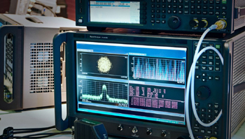
Figure 1 Example of scopes, signal analyzers and signal generators.
Essential T&M instruments and systems, as shown in Figure 1, include wideband spectrum analyzers and semiconductor automated test equipment (ATE). Wideband analyzers are used for visualizing RF signals, identifying interference and verifying design specifications, while ATE systems are used to verify functionality and performance of complex RF integrated circuits during manufacturing.
Modern wideband spectrum analyzers use advanced digital signal processing (DSP) combined with RF hardware and are used in wireless communications development, electronic surveillance and electromagnetic compatibility testing. ATE systems combine precise RF signal generation and analysis with digital test capabilities to evaluate mixed-signal devices like transceivers and systems on chips (SoCs). These systems are critical in ensuring quality in high volume semiconductor manufacturing.
NEXT-GENERATION REQUIREMENTS AND CHALLENGES
The evolution of next-generation wireless standards and the growth of high bandwidth applications drive the need for wider RF bandwidth spectrum analysis. This poses significant challenges for T&M systems, which must evolve to meet increasingly complex requirements.
Modern wireless systems are pushing toward multi-GHz bandwidths, particularly in mmWave and sub-THz applications. This necessitates T&M systems capable of capturing and processing unprecedented bandwidth in real-time. The challenge of processing a wider instantaneous bandwidth (IBW) involves designing high-speed RF data converters with sufficient resolution and implementing the massive DSP compute infrastructure required to handle the resulting data deluge.
The proliferation of multi-antenna, massive MIMO systems, beamforming technologies and high-throughput manufacturing tests are also driving increased demand for multichannel and synchronized testing. Next-generation T&M platforms must support a significant number of channels for testing multiple devices simultaneously to maximize test throughput and cost-per-test.
As wireless standards evolve, T&M equipment must adapt to changes, necessitating programmable DSP platforms and reconfigurable analog RF front-ends that can accommodate emerging modulation schemes and test methodologies without becoming obsolete.
Finally, a challenging aspect of meeting next-generation wireless/RF T&M system requirements is accomplishing all these advances while maintaining reasonable power consumption and physical dimensions.
LIMITATION OF T&M SYSTEMS
Conventional T&M systems with stand-alone data converters and discrete field-programmable gate arrays (FPGAs) cannot meet next-generation RF/wireless testing demands due to two critical bottlenecks.
First, the expanding instantaneous bandwidth requirements (now in multiple GHz) create data throughput challenges. High-speed JESD204C interfaces between converters and processors introduce signal integrity issues, complex PCB routing, reliability concerns and increased costs. Second, processing these wider bandwidths exceeds single-FPGA capabilities, forcing multi-FPGA solutions that create timing challenges, development complexity and thermal hotspots. The overhead of inter-FPGA communication wastes power and resources. While ASICs offer better integration and efficiency, they sacrifice flexibility and increase costs.
ADDRESSING T&M WITH A SINGLE-CHIP DEVICE
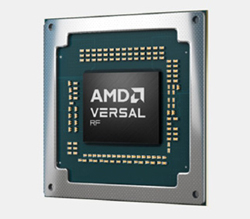
Figure 2 The AMD Versal™ RF Series.
Next-generation T&M systems require innovations in converter-processor integration, signal processing architectures, compute for high performance per watt and throughput to meet testing demands of advanced wireless technologies.
The AMD Versal™ RF Series, as shown in Figure 2, represents a paradigm shift in T&M system architecture, offering a single-chip monolithic solution by integrating data converters with heterogeneous computing resources, providing a platform designed for next-generation wireless testing.
Versal RF adaptive SoCs feature integrated 14-bit RF analog-to-digital converters (RF-ADCs) and RF digital-to-analog converters (RF-DACs) with built-in calibration capabilities that operate across a frequency range up to 18 GHz. This spectrum capability eliminates the need for multiple frequency conversion stages and external filtering. By integrating the converters into the SoC, Versal RF Series devices eliminate the need to use high-speed serial interfaces, which can reduce power consumption while simplifying board design. The scalable architecture supports various combinations of RF-DACs and RF-ADCs — up to 16 of each in a single package. This channel density enables multi-antenna testing, coherent multichannel applications and parallel device testing scenarios that would have previously required multiple discrete instruments or test modules. For semiconductor ATE applications specifically, this translates to higher throughput and lower cost-per-test. AMD Versal RF Series architecture, as outlined in Figure 3, incorporates multiple instances of commonly-used DSP functions as hard IP blocks, providing improvements in compute throughput and performance per watt. For example:
- Configurable 8-point to 4K-point 4 GSPS FFT/iFFT hard IP blocks enable real-time spectrum analysis of input signals with minimal latency
- Dedicated programmable polyphase filter bank channelizers separate wideband input spectra into narrow subchannels, critical for analyzing modern multi-carrier systems and can be used as generic FIR filters
- 8 GSPS configurable polyphase arbitrary resampler with up to 16,834 taps can be used as a generic polyphase filter

Figure 3 Architecture of the AMD Versal™ RF Series.
For flexibility and compatibility with existing IP, the programmable logic fabric includes DSP Engines (DSP58) supporting multiple data types, including single- and half-precision floating-point and complex 18 x 18 operations. This programmable capability enables adaptation to evolving standards and custom processing requirements.
With AI expected to transform T&M with advanced signal identification, anomaly detection and optimization capabilities, the integrated AI Engines in the Versal RF adaptive SoCs operate directly at the analog front-end, performing both traditional DSP and AI/ML inferencing without external transfers. This enables real-time interference detection, signal classification and anomaly identification — transforming test capabilities through intelligent measurement adaptation.
The architecture is complemented by a memory and I/O subsystem featuring LPDDR5X memory interfaces, 100G SerDes, 400GE networking and PCIe® Gen5 connectivity. This infrastructure, as demonstrated in Figure 4, supports the data movement requirements of modern test systems while maintaining interoperability with host systems and test environments.
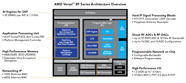
Figure 4 The operating system.
SUMMARY
Next-generation T&M systems need new architectures to address the requirements and challenges of ever-increasing RF bandwidth. AMD Versal RF devices integrate RF data converters, traditional FPGA programmable logic, dedicated DSP hard IP blocks and AI Engines to provide a flexible single-chip solution for the RF/wireless T&M market.
AMD
Santa Clara, Calif.
www.amd.com