

The ideal frequency synthesizer should preferably be broadband with fine frequency resolution, allowing the device to address many potential applications. Aside from frequency coverage and resolution, phase noise and spurs are critical parameters that impose the ultimate limit on the system’s ability to resolve signals of small amplitude. These requirements of wide frequency coverage, small step size and good spectral purity are the key drivers in the development of modern frequency synthesizers.1
SYNTHESIZER CHARACTERISTICS
Synthesizer characteristics depend heavily on a particular architecture.2 For decades, an indirect phase-locked loop (PLL) synthesizer was the most common and popular technique. As of today, PLL architectures still dominate. A generic single-loop PLL has the architecture shown in Figure 1. It includes a tunable voltage-controlled oscillator (VCO) that generates a signal in a desired frequency range. This signal is fed back to a phase detector through a frequency divider with a variable frequency division ratio, N. The other input of the phase detector is a reference signal divided down to a desirable step size. The phase detector compares the signals at both inputs and generates an error voltage. After filtering and optional amplification, the voltage slews the VCO until it acquires the lock frequency given by: ƒOUT = N ƒPD, where ƒPD is the comparison frequency at the phase detector inputs. Thus, the frequency tuning is achieved in discrete frequency steps equal to ƒPD by changing the division coefficient N.
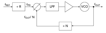
Figure 1 Functional diagram of a single-loop PLL synthesizer.

Figure 2 PLL spurs are located at multiples of the phase detector comparison frequency.
The main advantage of the PLL synthesizer is the excellent spur rejection resulting from the inherent lowpass filter capabilities of the loop. Note that the spurs are located at multiples of the phase detector comparison frequency and can be easily filtered out, as depicted in the diagram in Figure 2. However, this simple PLL synthesizer exhibits various limitations and tradeoffs. The main impact on the synthesizer performance is the reality of large division ratios required to provide a high frequency output with a fine resolution. Note that any noise generated by the PLL components is degraded at a rate of 20logN, where N is the division ratio. The division ratio is large in conventional integer-N PLLs operating at small step sizes because the step size must equal the comparison frequency at the phase detector. As a result, significant phase noise degradation occurs. Thus, this simple single-loop architecture suffers from mutually exclusive design goals.
Fractional-N synthesizers use fractional division ratios to break this coupling between frequency resolution and other characteristics. This allows a higher comparison frequency for a given step size. Fractional ratios are possible by alternating two or more division ratios, for example, N and N+1 and averaging the output frequency over a certain period.
Another way to look at this process is to calculate the number of pulses delivered by such a complex divider for a given time interval. The average division coefficient will be between N and N+1 depending on how many pulses are processed by each divider. The biggest concern associated with this scheme is that the instantaneous frequency at the fractional-N divider output is not constant. An abrupt change in the division coefficient leads to a phase discontinuity that produces a voltage spike at the phase detector output. Since the frequency division change occurs periodically with the same rate, it appears as discrete spurs in the synthesizer’s output spectrum. Furthermore, these spurs do not follow the integer relationship with respect to the phase detector comparison frequency and can be within the loop filter bandwidth. This situation is shown in Figure 3.
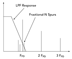
Figure 3 Fractional-N spurs can be located within the PLL loop bandwidth.
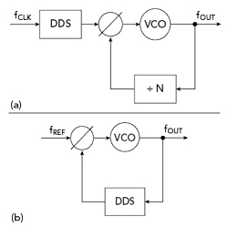
Figure 4 (a) DDS as a high frequency reference in a PLL synthesizer. (b) DDS as a fractional divider in a PLL synthesizer.
The direct digital synthesizer (DDS) is another effective solution to provide very fine frequency resolution without the standard penalty of the phase detector comparison frequency reduction. The DDS can serve as a fine-resolution, high frequency reference, as shown in Figure 4a, or be employed as a fractional divider, as illustrated in Figure 4b. While a DDS provides excellent frequency resolution, its spurious levels are usually quite high and do not follow the integer relationship. Moreover, the spurs further degrade because of the PLL multiplication mechanism. Although the two schemes in Figure 4 look different, they affect DDS spurs similarly. The ratio between the VCO output and phase detector comparison frequencies in both cases defines the overall loop division coefficient.
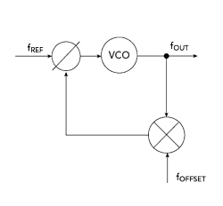
Figure 5 Frequency mixing improves PLL performance.
The synthesizer’s main characteristics can be drastically improved using frequency conversion (mixing) within the synthesizer feedback path, as shown in Figure 5. The idea is to convert the VCO output to a much lower frequency with a mixer and an offset frequency source. In specific scenarios, for example, when the operating frequency range is narrow, it is possible to eliminate the feedback frequency divider. In this case, the loop division coefficient equals one and no phase noise degradation occurs. However, inserting a mixer brings another spur generation mechanism due to the mixer intermodulation products. Unfortunately, these spurs do not follow the integer relationship either. They can also fall within the loop filter bandwidth, meaning the loop filter cannot filter them.
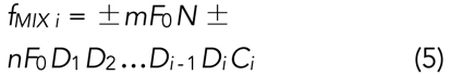
A clever solution is to use a chain of mixers within the PLL feedback path.3 Individual offset signals can be obtained from a standard high frequency variable reference using dividers and/or multipliers, as depicted on a general block diagram in Figure 6. In this block diagram, mixers M1 to Mi convert a VCO output signal to the phase detector comparison frequency, F0, equal to the synthesizer step size. The comparison frequency and mixer LO signals are produced from a common, high-stability and low phase noise reference signal using frequency dividers with frequency division ratios D1 to Di and frequency multipliers with multiplication factors C1 to Ci, respectively.

Figure 6 Mixer chain in the PLL feedback path.
A phase detector compares the signals at both inputs and generates an error voltage, which slews the frequency of the VCO to a lock frequency given by Equation 1:

After simple manipulations, the result is shown in Equation 2:

Since all the division and multiplication coefficients are integer numbers, we can write ƒ as Equation 3:

Where N = (D1D2...Di-1D1Ci± D1D2...Di-1Ci-1±...±D1D2C2±D1C1± 1) is an integer.
A desired output frequency can be chosen using an additional coarse-tuning divider with a programmable division ratio, N, inserted into the synthesizer loop. The divider loop provides a simple and reliable mechanism to pre-tune the VCO to the correct frequency. Then, the switch turns off the divider feedback path and connects the mixer chain to ensure no phase noise degradation occurs. An essential feature of this method is that the mixers do not generate undesired products within the synthesizer loop bandwidth. The output of every mixer includes many products, including the fundamentals of the mixer’s RF and LO signals and their harmonics, along with the sums and differences of the RF and LO and their harmonics. This relationship is given by Equation 4:

which can be written for the mixer, Mi, as Equation 5:
Assuming that all the coefficients are integers, the mixer products are given by Equation 6:

Where k is an integer number. Similarly, it can be shown that all harmonic and intermodulation products generated by the mixer chain are multiples of the phase detector frequency, F0, which a PLL loop filter can easily reject.
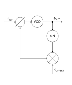
Figure 7 Inserting a multiplier into the PLL feedback path.
Moreover, the residual noise of the PLL can be further reduced by inserting a frequency multiplier instead of a divider into the feedback path. This architecture is depicted in the functional block diagram of Figure 7. Putting the multiplier within a PLL suppresses phase noise at a 20logN rate, operating exactly the opposite way to a frequency divider.
CONSTRUCTING A PLL
In general, there can be three basic scenarios for constructing a PLL. These are as follows:
- N>1: A frequency divider within the PLL loop (residual phase noise is degraded at 20logN)
- N=1: No division within the PLL loop (residual phase noise is not degraded)
- N<1: A frequency multiplier within the PLL loop (residual phase noise is improved at 20logN).
Thus, the proposed scheme allows minimal phase noise degradation beyond the fundamental 20logN rule. This keeps the integer relationship and phase-locked loops’ excellent spur rejection capabilities. Do we still need to break the integer relationship? If a design requires an infinitely small size, then yes, the integer relationship must be broken by introducing fractional-N or DDS techniques. However, in this case, it should be done within a relatively small band to fill in the gaps in the frequency plan. This certainly helps optimize the architecture and efficiently use other techniques, such as frequency up-conversion followed by frequency division, to minimize any additional spur intervention. Note that the phase noise of the available reference source still limits the synthesizer phase noise. Thus, having a reference with the lowest possible noise is essential in any frequency synthesizer architecture.
SUMMARY
The principles presented in this article can be highlighted to aid in modern PLL synthesizer design:
- Use integer-N techniques to employ PLL filtering capabilities for efficient spur suppression
- Use multiple conversions within the loop to minimize phase noise and spur degradation while keeping integer relationships for all phase detector and mixer products
- Use frequency multiplication within the loop for additional phase detector noise suppression
- Break the integer relationship at a single point with the smallest possible bandwidth, together with additional spur suppression techniques.
These principles are used in the Rubidium™ signal generator from Anritsu Company. This device demonstrates phase noise better than -140 dBc/Hz at 10 GHz output and 10 kHz offset and excellent spurious performance.4,5 Further improvements are possible using better reference sources such as sapphire-loaded cavity oscillators or optoelectronic methods.
References
- A. Chenakin, “Frequency Synthesis: Current Status and Future Projections,” Microwave Journal, Vol. 60, No. 4, April 2017, pp. 22–36.
- A. Chenakin, Frequency Synthesizers: Concept to Product, Artech House, 2010.
- A. Chenakin, “Low Phase Noise PLL Synthesizer,” U.S. Patent No. 7,701,299, April 2010.
- A. Chenakin, “Frequency Synthesizers Having Low Phase Noise,” U.S. Patent No. 11,817,871, November 2023.
- A. Chenakin, S. Ojha and S. Phadnis, “RubidiumTM Signal Generators Redefine Industry Standards for Spectral Purity and Stability,” Microwave Journal, Vol. 64, No. 11, November 2021, pp. 40–42.