
In last year’s November Microwave Journal article on components, Harlan Howe, Jr. authored an insightful and interesting article covering the history of microwave components. A whimsical Figure 1 depicted a dinosaur staring into the antenna of the first stone-age radar, while Figure 4 depicted a lady sitting on top of a high power WR-2100 waveguide diplexer that was several times her size. These images appropriately represent the birth of the microwave industry. These images also remind us of an undeniable trend in the industry: components are shrinking.
For 50 years after World War II the miniaturization trend was gradual with steps associated with solid-state and then surface-mount devices. More recently this trend is head spinning. We all benefit in our daily use of smaller commercial products. But military applications also benefit with greater functionality in smaller spaces. Advancements in this area are enabled by two primary factors: technology and integration. With small surface-mount devices, packaging and the clearance required for manufacturing consumes more space than the devices. This problem is solved for active circuits via integrated circuits (IC). Advancements in material technology now provide this option for passive microwave components. Manufacturers and users of passive components who do not embrace developing technologies ultimately risk the fate of the dinosaur.
Figure of Merit
Just as dizzying as the degree of miniaturization is the range of technologies that must be considered for a given application. Which of these technologies is best suited for a given application? In this article I’ll refer to inductors, capacitors, transmission lines and resonators as devices. I’ll refer to assemblies that use these devices such as couplers, splitters, phase-shifters, switches and filters as components.
Were it not for quality factor (unloaded Q, or Qu), devices could be as small as manufacturing allows. With today’s photolithographic techniques, that is small indeed. But unlike ICs, a primary factor that differentiates passive circuits and limits their performance is Qu, defined as the energy stored in a device divided by the energy dissipated. Energy is stored in a volume in some devices such as transmission lines, inductors and bulk quartz crystals, and in an area in piezoelectric surface devices. PWB and wafer area are viewed as limiting resources. Therefore, given the need for small size and good unloaded Q, one figure of merit (FOM) in passive devices could be Qu per occupied area. I will use Qu per square millimeter (Q/mm2) as that FOM.
Background
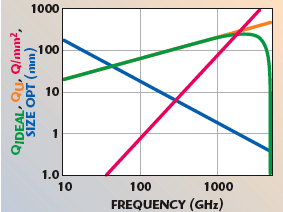
To fully understand this FOM, let’s step back and consider in more detail a foundational device for the microwave industry, the single-layer wire-wound solenoid. In Figure 1, plotted in brown is the computed Qu of a 1 mm diameter, 4 mm long, 10-turn copper-wire solenoid mounted vertically with one end grounded. The dashed curve is the ideal Qu ignoring parasitic capacitance. This curve is based on empirically derived data published by Medhurst2
Qu = 7.48dΨ![]()
where d is the solenoid mean diameter in millimeters, Ψ is a factor depending on the solenoid mean length to diameter ratio and f is the frequency in megahertz. Ψ ranges from about 0.5 to 0.9. Curve fit data for y is given in Rhea.3
For a given solenoid, Qu would rise continually with the square root of frequency were it not for parasitic capacitance. Medhurst also provided empirical data for solenoid capacitance and curve fit data is given in Rhea.3 For decades it was believed that the parasitic capacitance was inter-winding capacitance. However, it is primarily solenoid to ground capacitance.4 For this solenoid the capacitance is about 0.048 pF. For a vertically mounted solenoid, with increasing frequency, this capacitance increases the effective inductance and decreases Qu, as shown in the solid brown trace in Figure 1. The inductance approaches infinity and the Qu approaches zero at the resonant frequency of the low frequency inductance and parasitic capacitance. This causes Qu to peak at a frequency below the self-resonant frequency.
The solenoid capacitance is directly proportional to the solenoid diameter. To utilize a solenoid at higher frequency it is necessary to decrease the diameter and thus increase the resonant frequency of the solenoid. The approximate solenoid diameter in millimeters that results in maximum Qu is plotted as the blue trace in Figure 1. While the length to diameter ratio and wire spacing can be adjusted to maximize solenoid Qu, the most critical parameter is the diameter. At low frequency the optimum diameter may be larger than available space and at microwave frequencies the optimum diameter can be quite small. When so optimized, the maximum Qu of the solenoid is about 200. Plotted in red in Figure 1 is the Q/mm2 or FOM of the optimum sized solenoid. The FOM of the solenoid is proportional to ƒ2.
Sensitivity of Microwave Components to the FOM
The importance of device Qu varies among components. Hybrids, splitters, combiners, phase shifters, switches and other naturally broadband components have a high tolerance for relatively low Qu. Bandpass filters, oscillators, narrowband matching networks, high power and low loss networks require higher Qu.
Also, not all applications require small size. In certain applications, maximum Qu is more critical than Q/mm2. Bandpass filters with low loss requirements and percentage bandwidths less than five percent are a classic example. They often require relatively large machined cavities. The FOM is important when both size and Qu are important, which is an increasingly prevalent requirement. Other factors being equal, small size also means lower cost, particularly with high volume products.
FOM of Various Technologies
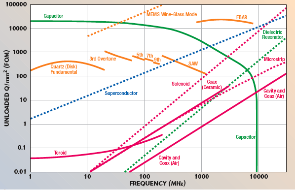
Plotted in Figure 2 is the unloaded Q per square millimeter (FOM) for various device technologies. Dashed traces represent unshielded or unpackaged devices and are therefore optimistic. Brown traces represent devices that are primarily limited by conductor loss. Red traces represent devices utilizing mechanical vibration.
First consider the green trace for an AVX U series NPO 1 pF 0402 chip size capacitor.5 At low frequency I estimated Qu is limited by the dielectric. At higher frequency Qu is limited by the effective series resistance (ESR) that is approximately 0.1 for this capacitor. Since the Ω reactance decreases with frequency, Qu decreases linearly with frequency from about 300 MHz to 6 GHz. Above 6 GHz Qu is limited by the series inductance of the capacitor and Qu falls to zero at the series resonant frequency. From this graph we see that at UHF and lower frequencies the FOM for the capacitor is very high. RF engineers can almost ignore Qu for capacitors but microwave engineers must be more careful. Nonetheless, the struggle for Qu with classic devices is with loss in the conductors of inductors, transmission lines and even capacitors.
The FOM for the solenoid is repeated from Figure 1. As the frequency increases the diameter of the solenoid is decreased. Notice that the solenoid has a higher FOM than all other technologies except superconductors and those utilizing mechanical vibration. This often comes as a surprise because we know that transmission lines and cavities can have higher Qu than inductors. This highlights an important consideration for this FOM graph. Inductors have a very high volumetric efficiency. Transmission lines yield higher Qu but only if they are large. Inductor Qu is limited because parasitic capacitance limits the maximum size. The high volumetric efficiency for the inductor explains the aversion to transmission line elements in ICs and low temperature cofired-ceramic (LTCC) components and the use of lumped elements in these devices. LTCC devices are covered later. The dashed trace indicates the data is for an unshielded solenoid. For components where component-to-component coupling is a minor issue such as splitters, or when the inductor is surrounded by capacitors, this is not a limiting factor. For filters with multiple inductors and needing high attenuation stopbands, inductors must either be shielded or widely spaced, so this data is optimistic. The FOM of the toroid is better than the solenoid at low frequency. At higher frequency hysteresis loss in the core becomes excessive.
Transmission line devices are represented by the cavity and coax, microstrip, superconductor and ceramic-loaded coax traces. The coax data is for a 75 Ω line with air dielectric and 10 μm metalization roughness. Both Qu and area decrease linearly with coax diameter so the FOM is essentially independent of coax diameter. The cavity data is for a square copper cavity with height equal to 1⁄2 each side and a cut-off frequency of 90 percent of the operating frequency. Interestingly, the FOM for cavities and coax are similar. Cavities possess higher Qu but also greater area. You might question utilizing area for coax and cavities but this was necessary to keep the data consistent. The microstrip data utilizes Arlon AD1000 0.508 mm thick substrate with electrodeposited copper.6 At low frequencies copper loss dominates and as with coax, the FOM is independent of substrate thickness. The microstrip data is unshielded and includes no margin for edge spacing. Again when surrounded by lumped elements, additional spacing may not be required. Otherwise this data is optimistic and the FOM is comparable to coax. An improved FOM is realized by loading the coax with high dielectric constant material. In this example Trans-Tech 9000 material is used.7 Essentially the FOM improves over air coax because the length shrinks as the square root of the relative dielectric constant, in this case the square root of 90.
The data labeled Superconductor is for a superconducting microstrip resonator on MgO substrate. The resistance of superconductors is zero only at DC. At 100 GHz the loss of superconductors and copper converge. However, over the plotted frequency range, the FOM is limited primarily by the substrate. The required cooling equipment would destroy the FOM and this data presumes a future day when room temperature superconductors are available. Superconducting filters are in use now not because of high volumetric efficiency but because of high Qu and therefore low loss in narrow band filters.
Since World War II, the high Qu and temperature stability of bulk piezoelectric quartz resonators have made them invaluable for excellent long- and short-term stability in oscillators and for very narrow band filters. Inexpensive resonators realize Qu over 100,000 and Qu exceeding 1,000,000 are readily available. Bulk quartz crystals are limited to an upper frequency limit of approximately 200 MHz but phase-locking offers both frequency extension and tunability for a plethora of communications devices. For data plotted in Figure 2, resonators are packaged in an HC 49/U metal case measuring 10.24 × 12.7 × 3.81 mm. The two large dimensions are used to compute the area for the FOM.
A well-proven technology that extends the upper frequency limit is piezoelectric surface acoustic wave (SAW) devices. They have been developed for resonators and monolithic filters with excellent shape factors and naturally flat group delay. The two large dimensions of a ceramic surface-mount 5 × 5 × 1.35 mm package are used for the FOM data.
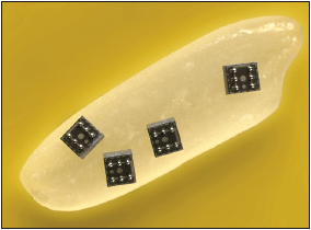
A new technology that has matured in this decade is the film bulk acoustic resonator (FBAR).8 Devices are similar to SAWs except sound energy is longitudinal. Typically a AlN piezoelectric thin film is used with non-standard IC processing techniques. FBARs have been used with great success for duplexers in wireless phones replacing ceramic loaded TEM mode diplexers. f(GHz) × Q for FBAR is approximately constant. For data plotted in Figure 2, an f(GHz) × Q of 4000 was used in a 0.4 × 0.5 mm wafer level package (WLP) at 1 GHz down to a size of 0.14 × 0.24 mm at 8 GHz. As can be seen, the FOM is two orders of magnitude better than ceramic-loaded TEM devices. Four FBAR WLP filters are displayed on a grain of rice in Figure 3. Many applications can be expected to arise from rapidly developing FBAR technology.
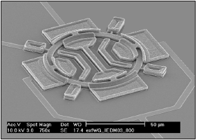
An even newer technology that has yet to see significant commercial application but that shows great promise is mechanical vibration devices constructed using MEMS processing. Multiple operating modes have been explored including miniature vibrating beams clamped on each end, beams free on the ends and contour mode disk resonators.9 These devices are currently limited to an upper frequency of approximately 200 MHz. A promising technology for higher frequencies is the wine-glass mode ring resonator. An example resonator is given in Figure 4. Data plotted in Figure 2 is for an unpackaged device. While this is significantly advantageous to the wine-glass mode resonator FOM, it should be considered that MEMS devices integrate directly into IC structures. Qu in air of 4550 has been achieved at 651 MHz and 2300 at 1470 MHz. Better results are obtained in a vacuum.10
Integration
The power of integration to reduce the size and cost of high volume products is undeniable. Integration of RF and microwave functions into ICs has historically been limited because of a poor FOM of inductors and transmission lines. The use of planar spirals in both MIC and MMIC has been only partially successful because the turn-to-turn magnetic coupling of the spiral is poor and planar structures have notoriously high parasitic capacitance.
The absence of LTCC technology in Figure 2 does not indicate unimportance. LTCC technology is missing because it embodies the implementation of many different technologies. LTCC devices are becoming more prevalent because they offer the ability to integrate inductors, transmission lines and other discrete devices on a substrate utilizing three-dimensional structures. The third dimension provides the option to create square cross-section solenoids. LTCC design guidelines also support closely spaced transmission lines to aid realization of tight couplers. The strength of LTCC is a degree of integration and miniaturization difficult to realize in MIC components.
Besides the vibration mode devices mentioned earlier, MEMS offers integration of classic microwave devices at the silicon level. MEMS can be used to create closed cavities, solenoids and other structures that are far more volumetric efficient than previously used planar devices. In the future, high volume applications will no longer need off-chip devices to realize high performance communications products. Over time, more microwave circuit designers will be IC designers.
References
1. H. Howe, Jr., “Passive Components: A Brief History,” Microwave Journal, Vol. 48, No. 11, November 2005, pp. 22–34.
2. R.G. Medhurst, “HF Resistance and Self-capacitance of Single-layer Solenoids,” Wireless Engineer, February 1947, p. 35, and March 1947, p. 80.
3. R.W. Rhea, HF Filter Design and Computer Simulation, Noble Publishing, Raleigh, NC, 1994.
4. R.W. Rhea, “A Multimode High Frequency Inductor Model,” Applied Microwave & Wireless, November/December, 1997, pp. 70–80.
5. www.avxcorp.com.
6. www.arlon-med.com.
7. www.trans-techinc.com.
8. R.C. Ruby, et al., “Thin Film Bulk Acoustic Resonators (FBAR) for Wireless Applications,” Proceedings of the 2001 IEEE Ultrasonics Symposium, Vol. 1, pp. 813–821.
9. H.J. De Los Santos, RF MEMS Circuit Design for Wireless Communications, Artech House Inc., Norwood, MA 2002, pp. 88–98.

Randy Rhea
10. Y. Xie, et al., “UHF Micromechanical Extensional Wine-glass Mode Ring Resonators,” Technical Digest of the 2003 IEEE International Electron Devices Meeting, 2003, pp. 953–956.
Randy Rhea is a graduate of the University of Illinois (1969) and Arizona State University (1973). His thesis was construction of an earth station that monitored Apollo 16 & 17 Unified S-band signals from the moon. He worked briefly at the Boeing Co. and Goodyear Aerospace and for 14 years at Scientific-Atlanta, where he became principal engineer. He founded Eagleware Corp. in 1985, recently acquired by Agilent Technologies, and Noble Publishing in 1994, recently acquired by SciTech Publishing. He has authored numerous technical papers, tutorial CDs and the books Oscillator Design and Computer Simulation and HF Filter Design and Computer Simulation. He has taught oscillator and filter design techniques to over 1000 engineers through full-day seminars at trade shows, the Georgia Institute of Technology and corporations. His hobbies include antiques, historical properties, astronomy and amateur radio (N4HI). He and his wife Marilynn have two adult children and reside near Thomasville, GA.