
Electromagnetic (EM) tools are indispensable for simulating high frequency designs, but they are poorly suited for synthesizing filters that require the determination of multiple parameters.

Randall Rhea
This article describes how to use EM simulation to aid a classic and under-utilized technique for filter design. The classic technique requires building prototypes of a few select resonators and plotting certain measured data. From these plots the filter dimensions are easily synthesized. Modern EM simulation breathes new life into this classic technique by eliminating the need to construct prototypes. This is particularly important when a process requires a long manufacturing cycle time. Unusual resonators such as compact planar, MEMS and multi-layer structures are increasingly used to solve challenging design requirements, but are poorly modeled by analytical formulas. The technique described here is particularly well suited for such structures.
The Classic Technique
The classic technique is also referred to as the general procedure, because it enables the design of bandpass filters of almost any type. This article emphasizes the application of EM to the procedure. Puglia1 gives a comprehensive description of the general procedure. For completeness, the procedure is briefly reviewed here.
Bandpass filters entail only three first principles:
- the resonators must exist,
- the resonators must couple to each other and
- the structure must couple to the terminations.
The general procedure is based directly on these first principles. The designer selects a form of resonator. Essentially, the only restrictions are that the resonator realizability and some method of coupling must exist. Next, data is acquired that relates the degree of resonator coupling to a variable parameter. Finally, data is acquired that relates termination coupling to a variable parameter. From this data, the filter is synthesized using simple analytical expressions.
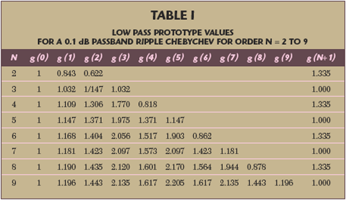
Filter tables are usually published in the form of prototype values for a low pass filter with 1 radian cut-off frequency and a source impedance of 1 Ω. An example for 0.1 dB passband ripple Chebyshev filters of orders 2 through 9 is given in Table 1. Many authors, including Puglia,1 provide simple formula for finding Chebyshev prototype values for other passband ripple and order criteria. g0 is the normalized source termination and gN+1 is the normalized load termination. Notice that for odd-order Chebyshev g0 = gN+1. For even-order, gN+1 increases for increasing passband ripple. There are N reactive values for an Nth order prototype.
The general procedure utilizes k and q values rather than low pass prototype values. k values relate to resonator couplings and q values relate to end-resonator loaded Qs. k and q values are easily derived from low pass prototype values.

As an example, the Chebyshev table with N = 5, q1 = q5 = 1.147, then k12 = k45 = 0.797 and k23 = k34 = 0.608.
These k and q values are normalized by the filter fractional bandwidth, bw.

where
fupper = passband upper cut-off frequency
flower = passband lower cut-off frequency
and

Then the actual filter couplings and loaded Qs are

Notice that the capitalized symbols refer to actual couplings and loadings while noncapitalized symbols refer to normalized values.
Determining a Structure’s K Values
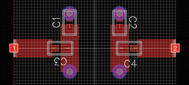
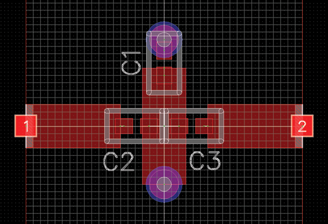
Consider the pair of resonators shown in Figure 1. The red areas are the microstrip metal, the blue areas are the via pads on the ground plane layer and the gray lines are the EM simulation grid. Each grid square is 15 mils on a side. The microstrip resonators are 90 mils wide and 240 mils long on a 31-mil thick PTFE-fiberglass substrate. The resonators are grounded with via holes at the bottom and are loaded with capacitors C1 and C2 at the top, thus forming a conventional combline. This metal layout pattern is simulated using the EMPOWER electromagnetic simulator in the GENESYS software suite.2 Test ports 1 and 2 are very loosely coupled to the resonators through input and output lines and very small capacitors C3 and C4. The edge-to-edge resonator spacing is 11 grid squares or 165 mils.
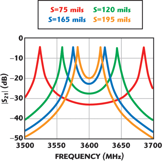
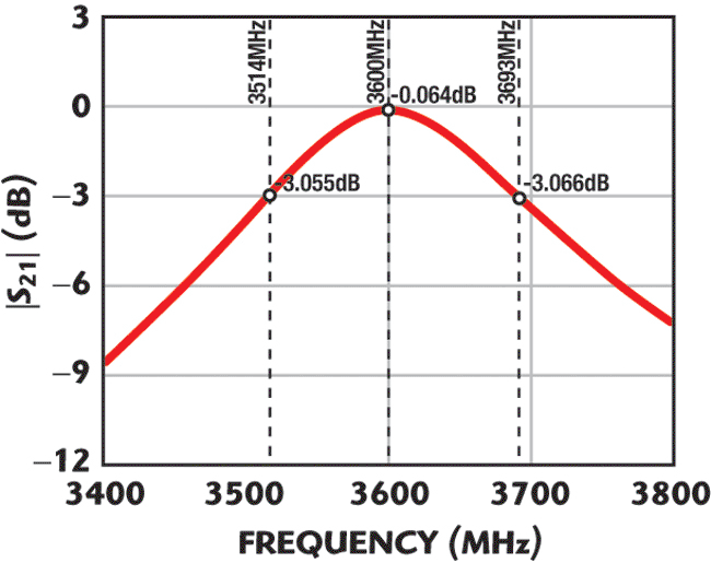
The frequency domain responses of this system are shown in Figure 2 for edge-to-edge spacings of 195, 165, 120 and 75 mils. C1 and C2 are tuned to center the response at the desired filter center frequency, in this case 3600 MHz. Two response peaks are observed when the loading coupling is very loose. The coupling coefficient of this system is given by

For the spacing of 165 mils, fupper = 3624.8 MHz and flower = 3575.2 MHz, so K = 0.0138.
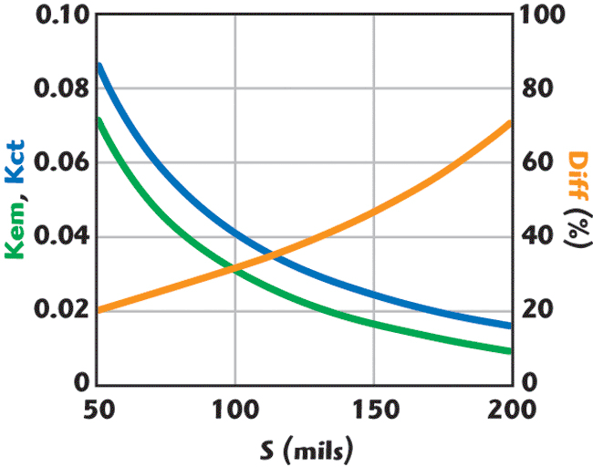
The general procedure involves plotting this data, as illustrated in Figure 3. The green curve is obtained by EM simulation, while the blue curve is the result of circuit theory simulation. The red curve is the difference, in percent, between these data. A feature of the general procedure is that K is typically a monotonic function of the variable parameter, and a smooth curve is easily drawn through a small number of data points. Here the data has been extrapolated to 50 and 200 mils. A plot of the coupling coefficient K for any spacing between these limits is now created.
Determining a Structure’s Q Values
Consider the resonator shown in Figure 4. The resonator is grounded with a via at the bottom and is loaded with capacitors C1 at the top. It is a single resonator identical to the coupled resonators. Test ports 1 and 2 are coupled to the resonators through input and output lines and capacitors C2 and C3 that control the loaded Q of each end resonator in the final filter. A frequency domain response of this system is shown in Figure 5, where the values of C2 and C3 are 0.3 pF. C1 is tuned to center the response at the desired filter center frequency each time a different value is tried for the coupling capacitors. The singly terminated loaded Q is given by

In this case fupper = 3693 MHz and flower = 3514 MHz, so Q = 40.2.
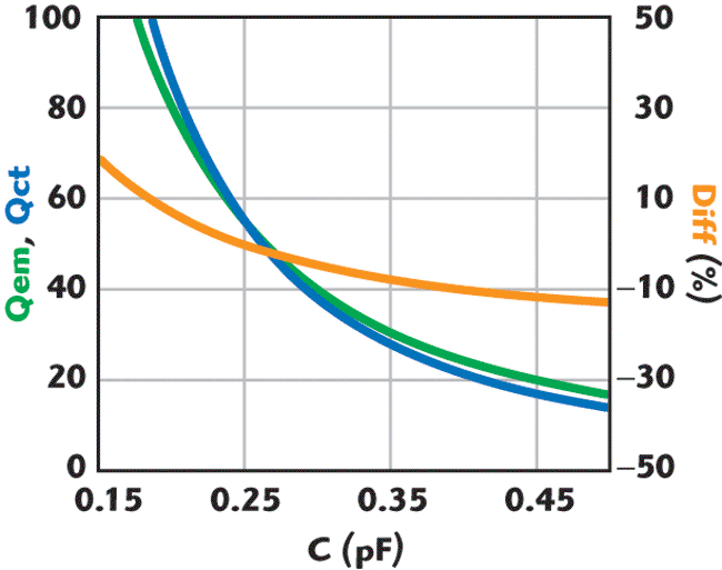
The general procedure involves repeating this data for a few different values of coupling capacitance. The Q was computed by EM simulation for capacitance values of 0.2, 0.3 and 0.45 pF. As was the case with K, the Q is typically a monotonic function of the variable parameter and a smooth curve is easily drawn through a small number of data points. Figure 6 shows the data extrapolated to capacitor values of 0.15 to 0.5 pF. The Q from EM simulation is shown in green, while the one obtained by circuit theory simulation is shown in blue. Their difference in percent is shown in red. A plot of the resonator loaded Q for any capacitance value between these limits is now available.
Designing the Filter with K and Q Data
The plots of coupling coefficient and loaded Q contain sufficient data to design on this substrate a 3600 MHz combline filter with any bandwidth, any order and any transfer approximation shape, provided only that the required spacings and capacitor coupling values fall within the given ranges. Consider, for example, a filter with the following parameters:
f0 = 3600 MHz
BW = 100 MHz
N = 5
Shape = Chebyshev
Ar = 0.1 dB
From Equations 1 through 9, it is found that Q1 = QN = 1.147/0.0278 = 41.29. From the green trace in the plot of Q vs. C, the required input and output coupling capacitors are shown to be approximately 0.28 pF. From the same equations, K1,2 = K4,5 = 0.797 × 0.0278 = 0.0222 and K2,3 = K3,4 = 0.608 × 0.0278 = 0.0169. From the green trace of the plot of coupling coefficient vs. spacing, the spacing between resonator 1 and 2, and 4 and 5, is approximately 120 mils, and the spacing between 2 and 3, and 3 and 4, is 150 mils.
Results Using the General Procedure
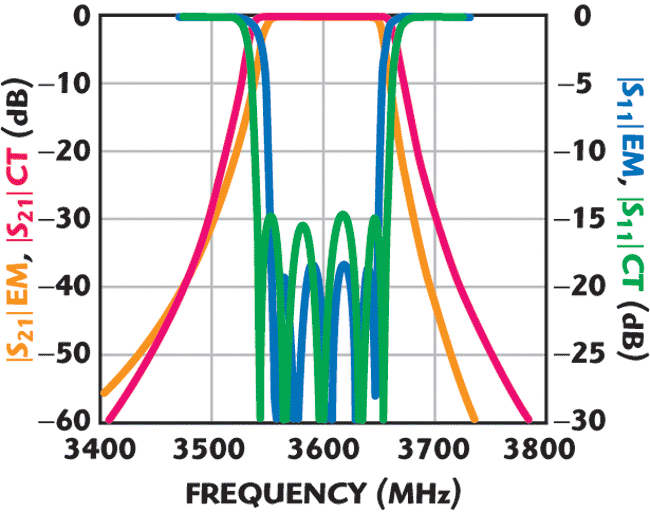
The layout of the final 3600 MHz combline bandpass is shown in Figure 7, with the dimensions given above. The EM and circuit theory computed responses are given in Figure 8. After EM simulation of the metal pattern, the loading capacitors C1 through C5 were optimized for the best response. The input and output coupling capacitors were fixed at the computed value of 0.28 pF. From the EM simulation, the resulting bandwidth is approximately 92 MHz, 8 percent lower than the desired 100 MHz, and the return loss is approximately 18 dB, 2 dB worse than desired. For comparison purposes, the circuit theory results show a bandwidth of approximately 116 MHz, 16 percent wider than desired and a return loss of only 15 dB, 5 dB worse than desired. Considering again the plot of coupling coefficient vs. spacing, the red trace is the percentage error of the circuit theory coupling with respect to the EM coupling.
Notice that, with a spacing of 50 mils the error is 25 percent, while with a spacing of 195 mils the error is 68 percent. This confirms the known phenomena in edge-coupled filters that a bandwidth error increases with narrow bandwidth filters. With wideband filters the error is often unnoticed while with narrow filters the error can be extreme.
There is another important lesson here. The failure of the circuit theory accuracy is obvious, yet there are only two resonators. This means that the error is not attributable to coupling between non-adjacent resonators, as is often believed.
The source of the circuit theory bandwidth error is evanescent modes. The effects of these modes are naturally considered by EM simulation but they are difficult to simulate using circuit theory, because their effect depends on the orientation and loading of the lines, the filter bandwidth and the substrate properties. The error increases with thicker substrates. Interestingly, inter-digital filters are far less susceptible to evanescent modes.
The design of filters, using EM simulation to find K and Q values, is more accurate than the design using circuit theory synthesis and simulation techniques. The simplicity of the math used to design this combline filter results naturally because the general procedure relies directly on the three first principles.
Second Example
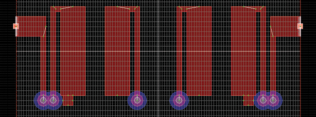
The layout of a four-section, 1672 to 1728 MHz bandpass filter is given in Figure 9, using a unique stepped-impedance resonator (SIR).3,4 SIR technology shortens the required physical length of the resonators by increasing the inductance of high current sections of transmission lines and/or increasing the capacitance of high voltage sections.
These quarter-wavelength 1700 MHz SIR resonators are 18.5 mm long on a 1.28 mm thick Rogers 3006 substrate with a relative dielectric constant of 6.15. The narrow sections of line are 0.5 mm wide and the wide sections are 2.5 mm. Conventional, 1.5 mm wide, unstepped quarter wave 1700 MHz resonators on this substrate are 20 mm long.
Folding also conserves space. The grid cells are 0.25 × 0.5 mm. This structure is poorly modeled using circuit theory transmission line models. However, it is a classic candidate for design using the general procedure, with EM simulation to find resonator couplings and end-resonator loaded Qs. Plotted in Figure 10 are the couplings and loaded Qs determined by EMPOWER.
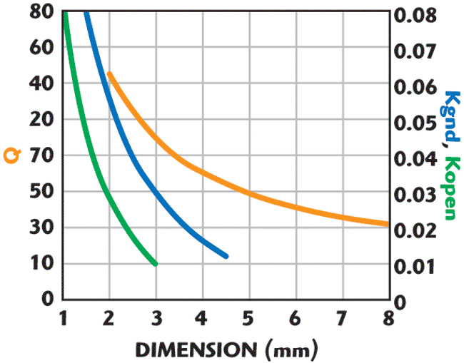
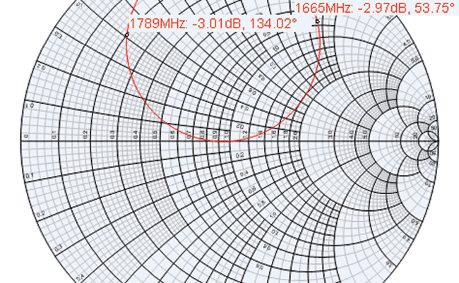
Notice that this SIR filter has two types of resonator couplings. Resonators one and two have lines that are open-ended adjacent to each other. The resonator coupling for this configuration is plotted in green, with the independent horizontal axis being edge-to-edge resonator spacing in millimeters. Resonators two and three have via grounded lines adjacent to each other. This coupling is plotted in blue. Plotted in red is the end resonator, singly loaded, Q vs. length of coupling line from the bottom edge of the input line to the centerline of the via. The left/right asymmetry of the SIR resonator precludes a doubly terminated measurement of the loaded Q, so an alternative method is used. For the EM simulation, a resonator is singly loaded and the resistivity of the metal is increased until the effective parallel loss resistance loads the resonator to a degree equal to the load termination. This occurs when the input return passes through the center of the Smith chart, as shown in Figure 11. The frequencies of the 3.01 dB return loss are then used in Equation 11 to find the singly terminated end-resonator loaded Q. For simulated coupling line lengths varying from two to eight millimeters, the required resistivity varies from 4.5 to 120. For the figure, a coupling line length of 5 mm and a resistivity of 75 were used. The input and output termination coupled-line transformers have the effect of slightly increasing the frequency of the end resonators. This was compensated empirically by adding small areas of metal to the end resonators, while examining the EM simulated response. The final SIR filter transmission and input return loss responses, computed by EMPOWER, are given in Figure 12. This filter occupies only about 40 percent of the space required by a conventional inter-digital structure. The general procedure and EM simulation are effective tool mates for quick and accurate design of filters with structures that are difficult to model analytically.
References
- K.V. Puglia, “A General Design Procedure for Bandpass Filters Derived from Low Pass Prototype Elements,” Microwave Journal, Part I, Vol. 43, No. 12, December 2000, pp. 22–38; Part II, Vol. 44, No. 1, January 2001, pp. 114–134.
- EMPOWER Manual, Agilent Technologies Inc.
- S. Yamashita and M. Makimoto, “Miniaturized Coaxial Resonator Partially Loaded with High Dielectric-constant Microwave Ceramics,” Transactions on Microwave Theory and Techniques, Part I, Vol. 31, No. 9, September 1983, pp. 697–703.
- R. Rhea, HF Filter Design and Computer Simulation, Noble Publishing, Raleigh, NC, pp. 116–121.
Randall Rhea is a graduate of the University of Illinois (1969) and Arizona State University (1973). His thesis was construction of an earth station that monitored Apollo 16 & 17 Unified S-band signals from the moon. He worked briefly at the Boeing Co. and Goodyear Aerospace and for 14 years at Scientific-Atlanta, where he became principal engineer. He founded Eagleware Corp. in 1985, recently acquired by Agilent Technologies, and Noble Publishing in 1994, recently acquired by SciTech Publishing. He has authored numerous technical papers, tutorial CDs and the books Oscillator Design and Computer Simulation and HF Filter Design and Computer Simulation. He has taught oscillator and filter design techniques to over 1000 engineers through full-day seminars at trade shows, the Georgia Institute of Technology and corporations. His hobbies include antiques, historical properties, astronomy and amateur radio (N4HI). He and his wife Marilynn have two adult children and reside near Thomasville, GA.