
Radar and electronic warfare (EW) have been the primary applications for extremely high-power transmitters, driving the demand for specialized high-power traveling wave tubes (TWTs) and magnetrons. Diminishing sources of TWT supplies, coupled with their poor reliability, inefficiency, large size and high total lifetime cost of ownership are causing a migration away from tubes. While improved pulse fidelity accompanies the shift to solid-state transmitters, next-generation radar depends on further improvements in waveform fidelity and flexibility.
Next-generation radar systems utilize long pulse widths, which present specific challenges. In response, Empower RF Systems has developed technology to reduce pulse distortion as a development step towards pulse shape matching, allowing the reproduction of the input pulse without distortion. The pulse correction is performed within the amplifier in real-time. This is important because long pulse width radar is especially vulnerable to over/undershoot and droop, which can be eliminated to extend radar range and reduce receiver target acquisition time. The benefits from an EW perspective are the ability to accurately mimic adversarial pulses without pre-processing, allowing precise threat simulation and spoofing.
THE PRIMARY CAUSE OF DROOP IN SOLID-STATE POWER AMPLIFIERS (SSPAs)
This article discusses the correction of pulse droop and rising edge overshoot with data from Empower’s 40 kW L-Band long duty cycle liquid-cooled pulsed amplifier, Model 2237, shown in Figure 1. The primary cause of droop in a GaN power amplifier is the thermal response of the transistor. GaN has an inverse gain relationship with temperature. The thermal response of the transistors reduces the gain by 0.5 to 1.0 dB, depending on the temperature rise during the pulse. The droop is compounded with cascaded transistors resulting in a further reduction in output power. This is summarized in Figure 2. The second contribution relates to a power supply’s ability to source current at high frequencies. During the pulse, the capacitive energy across the drain of the transistor discharges. This starts at the leading edge of the pulse and as the pulse progresses to the trailing edge, the gain is increasingly reduced by the resulting drop in drain current and drain voltage. These two factors can account for up to 3 dB of droop. Fixing the droop using software allows a reduction in the size and complexity of the power supply and increases average transmit power. The result is improved size, weight and power (SWaP), cost and MTBF.
Figure 1 Model 2237 L-Band 40 kW Pulsed Transmitter.
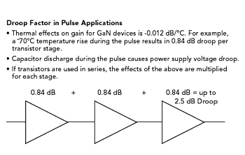
Figure 2 The impact of cascading stages.
PULSE PARAMETERS AND IMPACT ON RADAR PERFORMANCE
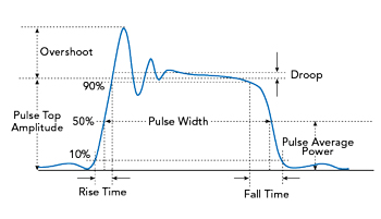
Figure 3 Pulse parameters.
Pulse droop is defined as the distortion of a flat-topped rectangular pulse, characterized by a decline of the pulse top. Figure 3 describes the characteristics of a pulsed signal. Generally, each pulse includes an overshoot and ripple at the leading edge of the pulse and a pulse droop, which is the reduction in the amplitude between the beginning and end of the pulse.
THE IMPACT OF OVERSHOOT AND DROOP ON RADAR PERFORMANCE
A radar transmitter will have a limiter to protect the amplifier output stages from exceeding the peak power ratings. When overshoot is present, the gain must be set so the overshoot of the pulse does not activate the limiter. When overshoot is absent or minimized, the amplifier output can be set just shy of the limiter threshold. In the case of droop, the power during the pulse is dropping over time, further reducing the average power. By examining the radar range equation, the impact of reduced power can be seen in Equation (1).

Where:
Rmax = the maximum range
Pt = the transmitter power
G = the transmitter antenna gain
σ = the target’s radar cross-section
Ae = the receive antenna effective aperture
Smin = the minimum detectable signal.
Assuming all other terms remain constant, the maximum range varies as the fourth root of the transmitter power. For example, a 1 dB improvement in average power increases the range by 6 percent.
PULSE CORRECTIONS
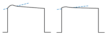
Figure 4 Illustration of the pulse droop correction of RF output.
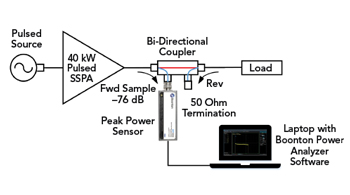
Figure 5 Test setup.
Figure 6 Output power coupling.
Each of the two main sources of droop has a repeatable response in time. These are typically marked from the leading edge of each pulse. With fast enough sample rates, an algorithmic solution exists that can change the amplifier gain throughout the pulse in real-time.
As an example, let’s take the simplest form of the algorithm. Since the junction temperature rate of change is highest on the rising edge of the pulse when the transistor is turning on and conducting, the adjustment to the gain at the beginning of the pulse must be greater than during the remainder of the pulse. Implementing this will result in a significant reduction in overshoot. The expected result of this simple adjustment is shown in Figure 4.
After the overshoot section, gain adjustment of the algorithm can be employed as a second element. The math is simple; the droop has a slope, so the gain adjustment simply adds in the inverse gain slope. The applied algorithm repeats itself with each pulse. This two-step algorithm can be further refined by adding more adjustment points, however, the results of a two-stage correction are very good and are shown later. The correction algorithm resides in the FPGA firmware and contains a finite-state machine described in HDL. The correction algorithm is configured with the appropriate parameters from a digital calibration process performed at the factory. The parameters include the slopes of the two-stage corrections and the initial power level at the leading edge of the pulse.
TEST SETUP (refer to Measurement Considerations below)
For demonstration, an Empower amplifier is driven with a 1.5 GHz, 500 μsec pulse, nominally at 0 dBm. A separate guard band input is used to frame the pulse for operating in true pulse mode. The amplifier is set to full gain, achieving 40 kW peak power at the output. The overall setup is shown in Figure 5.
The amplifier has a bidirectional coupler at the output as seen in Figure 6. The coupling factor is 76 dB. A Boonton RTP5006 USB real-time peak power sensor was used because this is the only sensor fast enough to capture the peak of the overshoot. The full power is terminated into a 50 Ω load.