
With communication systems evolving quickly, the main challenge for manufacturers is to design intelligent, secure and energy-efficient systems. This development is driven by the traffic generated by the various uses of mobile communications and new associated applications, necessitating the frequent introduction of new technologies to meet these requirements. The arrival of the new 5G standard has brought a radical change in the architecture of base stations with the development of active antenna systems (AAS).
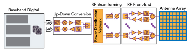
Figure 1 Active Antenna System architecture.
To understand the complexity of these new communication systems, Figure 1 shows an abstract high-level representation of the system where the problem is broken down into three parts:
- The antenna made up of many radiating elements
- The RF front-ends composed of various analog functions (like power amplifier (PA), low noise amplifier (LNA), mixer, filter and phase shifter)
- The digital modules that manage the signal processing (DSP), the beamforming control algorithms, and the non-linearity compensation of the RF circuits (DPD).
This system’s design decomposition results in the interaction of several specialized teams with various levels of maturity (R&D or production, for example) and in an asynchronous design time. Controlling the cost of the overall project can be challenging if a dependency exists between these teams. For example, the sizing and adjustment of the PA linearization system entrusted to the DSP team can only be made when the circuit team produces the PA. Thus, these cascaded tasks that are required for the prototyping of certain elements result in a long time to market.
If the overall system does not meet the targeted specifications due to poor coordination between teams, very costly and time-consuming testing and adjustment phases may be necessary after the demonstrator has been manufactured. This cycle of development and production is illustrated in Figure 2.
TOP-DOWN DESIGN FLOW
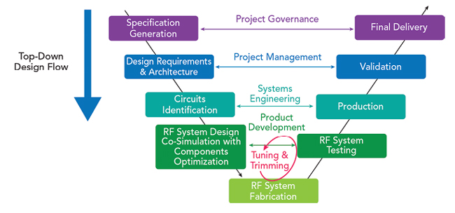
Figure 2 V-Model design cycle based on experimentations.
In Figure 2, the “Top-Down” design flow of the system consists of breaking down the system’s global specifications into sub-specifications. The work of the system architect then consists of defining the sub-specifications of each circuit, making up the overall solution by balancing the constraints on each block as well as making it possible to optimize the design and production costs of the entire chain.
The more the specifications targeted for an element of the chain are restrictive, the more the cost of this circuit is important. The system architect indicates which specific circuits have to be developed and which circuits are already available on the shelves that have to be integrated.
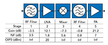
Figure 3 Preliminary system simulation made during the V-design cycle.
The sizing of each circuit is therefore very important. Theoretical models of each circuit can be used to pre-estimate the overall performance. Thus, the optimization of the communication system design requires simulation tools to evaluate and validate the global performance with more or less theoretical models indicating the gain, the noise factor or even the linearity criteria of each element (see Figure 3).
Different options are available to the production team once each circuit composing the system has been used. The historical method is to conduct a first system assembly and see if it meets the targeted specifications. Depending on the sophistication and complexity of the signals processed by the chain, optimization and engineering phases are necessary to achieve the desired performance, as illustrated in the feedback loop in Figure 2. Depending on the system’s complexity, each iteration can represent several months of work and hundreds of thousands of dollars, or even more if it is an active antenna composed of several thousand elements.