
Another important parameter is the figure of merit (FoM) for high performance, high-power switches (Ron*Coff/VBV). Where Ron is ON resistance of the switch, Coff is the off capacitance and VBV is the breakdown voltage. The lower the number, the more superior the technology. Tagore’s second generation of GaN technology has a FoM of 3 fs/V. As technology matures and improves, the FoM should improve further with newer generations, enabling further improvements in the switch performance.
GaN VERSUS PIN DIODE RF SWITCHES
Tagore’s GaN RF switches are designed with depletion mode GaN HEMT technology. The GaN HEMT with a high breakdown voltage has a saturation current close to 1 A/mm, so a 2 to 3 mm device theoretically meets the peak current requirement for 100 W of power in a 50 Ω system. The switch function is like a silicon on insulator (SOI)-based switch where the device is turned on/off by applying voltage at the gate terminal. Unlike SOI, however, where the breakdown voltage is very low, typically around 3 V, the breakdown voltage of a GaN device is very high.

Figure 5 PIN diode (a) and GaN (b) SP4T RF switches.
A high-power switch can be realized without stacking many devices in series, which is critical for reducing Ron and Coff. Because the devices are in depletion mode, they require negative voltage to turn them off and zero volts to turn them on. All Tagore switches are designed with a controller die co-packaged with GaN die. The controller generates gate voltage signals to control all the GaN devices. Negative voltage is generated inside the controller, so it requires only a minimum 2.7 V (5.5 V maximum) supply and a 1.2 V (5.25 V maximum) logic signal to control the RF switch state. The only external component necessary is a bypass capacitor on the charge pump pin, as shown in Figure 5.
Unlike GaN RF switches, PIN diode-based RF switch design is much more complex and requires many iterations to implement and optimize. Performance is heavily dependent on the parasitics associated with external components and board layout as many passive biasing devices are connected to the RF signal path. PIN diode control requires both high current and high voltage. The ON state resistance of the PIN diode is a function of bias current, where OFF state power handling is controlled by applying a high reverse bias voltage. It requires high forward bias current, in the range of 200 to 400 mA for 100 W switch, and high reverse bias voltage, in the range of 140 V.
Figure 5a shows a typical implementation of a PIN diode-based SP4T 100 W switch with the lowest operating frequency of 50 MHz. The figure shows the bias condition when the RF1 path is ON. To keep the ON resistance low, the ON path diode is biased at 400 mA, shown with red fonts and arrows. The OFF path shunt diodes are biased at 25 mA and the series diodes are reversed biased at 140 V. The ON state bias power requirement is 2 W (5 V × 400 mA) and the OFF state bias power requirement for each path is 3.5 W (140 V × 25 mA). The total DC bias power requirement to bias the 4T switch is 12.5 W. The majority of biasing power is dissipated in bias resistors, thus they must be capable high-power dissipation. Additional boost circuitry is required to generate the high voltage to reverse bias the diodes from low supply rail.
As shown in Figure 5, the PIN diode requires 32 passive components, not counting the boost converter circuit, while the GaN-based switch can be realized with 3 V and 200 uA current, or 0.6 mW total power consumption and two components. As RF ports are 50 Ω without any passive components connected, the design can be implemented and ported to any board, eliminating the design complexity associated with the diode switch.
GaN-based solutions require board space on the order of 1/10 of PIN diode designs—3 × 3 to 5 × 5 mm—and DC power dissipation is almost zero, which reduces heat sink requirements, further reducing overall size and weight. The MIL-COM radio RFFE shown in Figure 1 would require 176 components for a PIN diode solution, not including components for high voltage boost circuit, versus seven switches and seven capacitors for a GaN-based solution.
GaN RF SWITCH PERFORMANCE
The following examples from Tagore Technology’s portfolio of GaN RF switches with integrated controllers will illustrate the performance capabilities of GaN. Figure 6 shows the performance of its TS8021N 2T switch. Figure 6(a) and 6(b) show the small signal performance. It has a very low insertion loss (IL) of 0.2 dB at 1 GHz and less than 0.5 dB up to 4 GHz. Figure 6(c) shows that the switch has a PCW_0.1 dB of 50 dbm (100 W). Harmonic performance is better than 80 dBc up to 90 W of power as shown in Figure 6(d). The 5 × 5 mm QFN package requires only one external capacitor. The switch is ideally suited for a high-power manpack, trunk mount radio application.
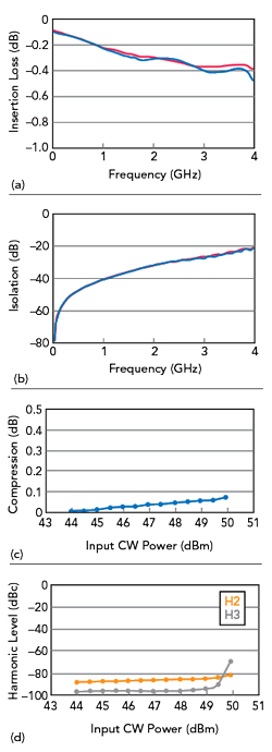
Figure 6 TS8021N switch performance: insertion loss (a), isolation (b), compression (c) and harmonics (d).
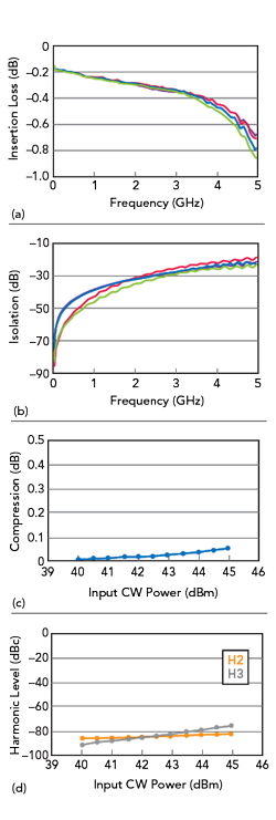
Figure 7 TS8242FK switch performance: insertion loss (a), isolation (b), compression (c) and harmonics (d).
Figure 7 shows the performance of a TS8242FK, 4T switch with a PCW_0.1 dB of 30 W, ideally suited for filter bank fanout, as shown in Figure 1, for portable 10 W LMR/PMR or military communications radios. The switch has 0.3 dB IL at 2.5 GHz and harmonic performance is better than 85 dBc at 10 W.
TS8329FK switch performance (see Figure 8) is designed for a fail-safe function in massive MIMO (mMIMO) base station applications. The switch has 0.5 dB Rx IL and 35 dB isolation in the newly released 5G C-Band. It has a PPEAK_0.1 dB of 100 W and a switching time of 0.5 uS. Both TS8242FK and TS8329FK switches are integrated in small 3 × 3 mm QFN packages with only one external capacitor saving significant board space compared to PIN diode solution.

Figure 8 TS8329FK switch performance: insertion loss (a), isolation (b) and compression (c).
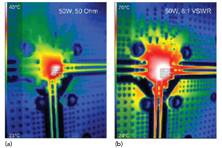
Figure 9 TS8021N switch temperature profile when matched to 50 Ω (a), with an 8:1 VSWR (b).
High-power switches are expected to withstand very harsh conditions in terms of VSWR, especially switches close to the antenna. GaN RF switches have excellent thermal and VSWR performance. Figure 9 shows the thermal performance of a TS8021N switch with 50 W of input power into 50 Ω (see Figure 9a) and with an 8:1 VSWR (see Figure 9b). The thermal image is taken after the part is exposed to this condition for 1 minute. VSWR is shown for the worst condition, in terms of power dissipation, which happens in the low impedance state. The temperature in the opposite condition, worst in terms of peak voltage, is much lower and can be easily withstood because of the characteristic high breakdown voltage of GaN devices.
SUMMARY
High-power front-end design using GaN switch technology has been demonstrated. GaN RF switches address major challenges associated with board space and SWaP in tactical military communications and base station radios. GaN switch technology eliminates the complexity associated with PIN diode switches for RF design engineers and makes the design portable, which is critical for mMIMO and phased array architectures, given that Tx and Rx array size continues to grow. With further technology advancement and improvements in the FoM, newer generations of GaN-based switches will open the door for many applications, such as high-power tunable matching circuits, tunable antennas and tunable filters.