
GaN RF switch technology enables the efficient realization of modern high-power multi-band radios in terms of size, weight and power (SWaP) while significantly reducing complexity.
PIN diode technology has been the historic choice to realize the RF switch function in RF front-end (RFFE) high-power radio design. This technology was adequate as the number of frequency bands were limited and board space was not a constraint. Modern high-power base stations and tactical military communications radios, however, are required to cover many bands to meet demand for secure voice and data communication while optimizing SWaP.
5G base station remote radio head (RRH) design is becoming extremely complex, driven by mMIMO architectures, where many RFFEs must be implemented in limited board space. RRH units are typically mounted on tall poles, which adds additional constraints in terms of total size and weight to ease installation and maintenance of base station equipment. RFFE efficiencies and total loss budgets are also critical to manage total thermal dissipation. Lower loss in front-end filters and RF switches helps reduce total power loss and relaxes heat sink requirements, which also reduces RFFE size and weight.
High-power phased array radars are like 5G base stations, where many RFFEs are required to be integrated in a limited board space. It is becoming prohibitively difficult to realize multiple frequency bands and multiple RFFEs distributed over a wide frequency range with traditional PIN diode switch technology due to the complex biasing schemes and numerous passive components required. New RF switch technology can help solve many of these issues.
TACTICAL MIL-COM RFFE REQUIREMENTS
Figure 1 represents the typical dual power amplifier (PA) RFFE lineup of tactical military communications radio. The dual PA architecture, normally with GaN-based PAs, is most common, covering a broad frequency range of 30 MHz to 2.6 GHz. Continuous frequency coverage is essential in many proprietary military software-defined radios covering 30 MHz to 2.6 GHz, for a 6.5 octave bandwidth; thus, a theoretical minimum of seven bands are needed.
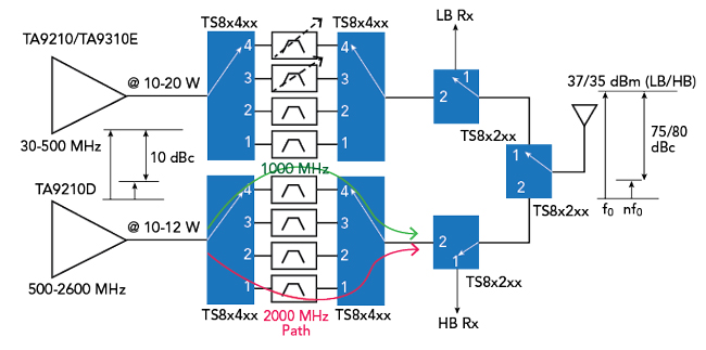
Figure 1 Dual PA front-end for a tactical military communications (MIL-COM) radio.
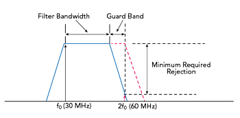
Figure 2 Harmonic filter requirement for the tactical radio.
A harmonic filter, however, requires a guard band to achieve the minimum required rejection for second harmonics of the lower end of the frequency within the band. For example, as shown in Figure 2, the first band cannot be 30 to 60 MHz, or one octave, since the second harmonic of 30 MHz falls within the band. The first band must be 30 to 50 MHz, assuming a 10 MHz guard band to achieve the desired filter rejection to meet harmonic rejection requirements.
With a minimum 10 MHz guard band, frequency range must be split into eight discrete bands to have continuous coverage from 30 MHz to 2.6 GHz. The main function of the RF switch in this lineup is to route the RF signal to the appropriate harmonic filters and combine the signals, again, after passing through the harmonic filter to route them to the antenna. Performance of the RF switch is critical to the radio’s overall performance.
Switch insertion loss is one of the most important specifications to reduce total power dissipation. Lower insertion loss of the switch also reduces total power required from the PA. A reduction in PA output power lowers PA DC power consumption, one of the biggest contributors to a system’s total DC power requirement, thus improving the talk time of battery powered portable radios, which is crucial in mission-critical applications. Reduction in power loss, and thus total thermal dissipation, also helps reduce the size of the heat sink which in turn helps reduce the total size and weight of the radio, which is also very important in many military communication applications.
The second key specification is switch harmonic performance, especially switches which are used after the harmonic filters. Land mobile/private mobile radio (LMR/PMR) is specified to meet a 75 to 80 dBc harmonic requirement at rated power. PAs are operated deep into saturation for better efficiency, where harmonic levels are in the range of 10 to 20 dBc. Thus, harmonic filters are required to provide a minimum of 60 to 70 dB rejection to meet regulatory requirements.
For military radios, switches used after harmonic filters do not have the benefit of harmonic filter rejection, thus their harmonic performance needs to be better than the overall requirement to meet the total transmit (Tx) lineup requirement. Based on the harmonic performance of the PA+ filter, the harmonic performance of switches must be better than 80 dBc to meet regulatory requirements.
Figure 1 also demonstrates another critical issue associated with switch isolation. Isolation of switches at lower frequencies is typically very high, so it is not an issue; however, it could pose a problem for higher bands. The second harmonic of the 1 GHz signal path, shown by green arrow in Figure 1, for example, could pass through the 2 GHz signal path, shown by the red arrow. The 2 GHz path harmonic filter does not provide any rejection, thus combined input and output switch isolation must be higher than the rejection provided by harmonic filter to meet the overall harmonic requirement.
BASE STATION AND RADAR RFFE REQUIREMENTS
Figure 3 represents the lineup of a typical base station or RRH unit. Modern 5G base stations use mMIMO architectures for electronic beam steering, requiring many RFFEs depending on the number of transmitters and receivers in the array. High-power phased array radars use similar architectures as well.
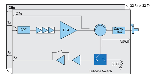
Figure 3 Notional RRH front-end.
In both applications, RF switches provide a fail-safe function to protect the receiver in the event of a poor VSWR condition from the antenna. In the event of poor VSWR, due to damage or an object, such as a bird blocking a portion of the antenna aperture, Tx power reflects back to the radio during transmit. In the absence of a fail-safe switch, high reflected power could damage the sensitive receiver. A fail-safe switch is added in the receive (Rx) lineup to address such scenarios.
The fail-safe switch is switched to the Rx port during the Rx time slot and to the Tx port during the Tx time slot. In the event of high VSWR during Tx, the switch routes the reflected power coming from the antenna through a circulator to a 50 Ω load connected at the Tx port of the switch, thus protecting the receiver from high power.
Key RF switch requirements for the fail-safe application are low insertion loss in Rx and high power handling in Tx. During the Rx time slot, the switch falls in the Rx path, thus its loss directly impacts the overall noise figure and thus sensitivity of the receiver. During Tx, the switch must handle the maximum transmit power in the event of poor VSWR and provide high isolation to the Rx port.
The system is designed to detect poor VSWR conditions, however a switch must handle high power until the system detects a fault condition and reduces Tx power or turns-off the transmitter. This duration is typically 10 seconds before the system reacts, thus the switch needs to handle high power without damage during this interval.
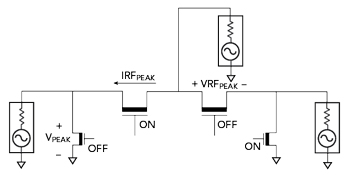
Figure 4 GaN RF switch.
Typical isolation varies from 25 to 35 dB depending on the maximum peak power of the transmitter and maximum power handling capability of the low noise amplifier. The switching time requirement for a base station application is less than 1 us. For radar, the switching time requirement is more stringent as it directly impacts radar range.
GaN RF SWITCH TECHNOLOGY
GaN’s benefits in high-power PAs are well known. A wide bandgap GaN device has a high power density due to its high breakdown voltage and high carrier density. GaN’s benefits in high-power switch technology are not as well known; however, the properties of GaN that improve PA performance apply to the realization superior high-power RF switches as well.
As shown in Figure 4, there are two requirements for RF devices used in high-power RF switches. The ON arm of the RF switch must handle very high RF current, where the OFF arm must handle very large RF voltages. Table 1 lists peak RF voltage and current requirement versus RF power for RF switches.
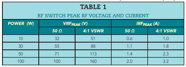
For example, 10 W of RF power generated in a 50 Ω system produces 32 V peak and 600 mA of peak current. With a 4:1 VSWR, which is typical for the front-end section of a radio, a switch must handle more than 50 V peak and 1 A of peak current. For 100 W of RF power generated, a switch must handle 160 V peak and 3.2 A of peak current. RF switches, therefore, must handle high voltages and currents. These are key characteristics of wide bandgap devices such as GaN, and the same properties exploited to design high-power GaN PAs.