
Time-division duplex (TDD) schemes enable 5G wireless systems to deliver next-generation performance. This article explores the essential capabilities for test instrumentation to characterize the performance of high speed switches in 5G TDD networks.
TDD is a type of duplex communication where uplink and downlink transmissions share a single frequency band, organized by rapidly interchanging time slots. For comparison, an alternate duplexing scheme known as frequency-division duplex (FDD) uses two separate channels for uplink and downlink transmissions. A sufficient frequency gap between the two is required to avoid interference between the transmitter and receiver.
While FDD is widely used, it demands more spectrum than TDD, contains a portion of unusable spectrum for adequate channel separation and must abide by predetermined allocations of uplink/downlink network resources. Due to these factors, TDD is becoming a more favorable option for 5G network applications, especially at high mmWave frequencies. TDD brings efficiency to spectrum management and can accommodate asymmetric traffic, enabling dynamic bandwidth allocation of high-band frequencies in dense 5G network deployments.
Successful TDD implementation requires superior synchronization and fast, efficient and precise switching components—typically operating in the microsecond or nanosecond range—to avoid latency and timing overlap. These timing requirements become more stringent as applications move up in frequency.
SWITCHING SPEED AT HIGH FREQUENCIES
In 5G TDD systems, each frame has a fixed 10 ms duration and is divided into subframes with fixed 1 ms durations. Subdividing even further, each subframe is broken into different slots that contain a cyclic prefix and several orthogonal frequency-division multiplexing (OFDM) symbols. Classifications of TDD OFDM symbols include uplink, downlink and flexible symbols that can be assigned as either uplink or downlink. Special guard periods are used to prevent interference. Guard periods need a sufficient duration to accommodate receiving the downlink data and switching to the new uplink assignment.
Slot duration and the number of slots per frame are variable. Typically, when operating at higher mmWave frequencies, the subcarrier spacing widens as the slot length shortens. To illustrate this, Figure 1 shows a 15 kHz subframe containing just one slot that takes up the full 1 ms allotment. Moving up to a 60 kHz subcarrier spacing reduces each slot’s time to 0.25 ms, and even further to 0.0625 ms with a 240 kHz subcarrier spacing. For reference, FR1 frequencies use 15, 30 and 60 kHz subcarrier spacings, while higher FR2 frequencies use 60, 120 and 240 kHz subcarrier spacings. Consequently, shortening the slot length also compresses OFDM symbol length, which can dip into the sub-microsecond time range.
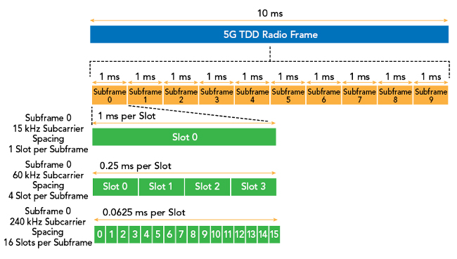
Figure 1 10 ms 5G TDD radio frame showing 1 ms subframes and subframe 0 slot configurations at 15, 60 and 240 kHz subcarrier spacing.
With uplink/downlink handover occurring at the symbol level, components tasked with switching between rapidly interchanging uplink and downlink assignments must operate at the proper speeds, especially in high frequency applications.
Switching speed is defined by the elapsed time interval between a switch’s on/off state or off/on state, and key parameters for defining switching speed are rise time and fall time. As defined by IEEE, rise time is the time it takes a signal to change from 10 to 90 percent of the signal magnitude, i.e., the time interval from the first crossing of the proximal line to the first crossing of the distal line. Similarly, fall time is the time it takes a signal to change from about 90 to 10 percent of the signal magnitude, i.e., the time interval from the last crossing of the distal line to the last crossing of the proximal line.
Since rise time is a key metric in quantifying switching speed, TDD switches require test equipment with exceptional rise time capabilities for proper analysis. Diode-based peak power sensors use low-impedance loads across the smoothing capacitors so they can discharge rapidly when there is a drop in RF amplitude. Coupled with a small smoothing capacitance, an RF peak power sensor can attain a very fast rise time. Leading-edge power measurement instruments have 3 ns rise time capabilities, enabling the reliable capture of 5G TDD switching components. Interestingly, sensors with these fast rise times also have 195 MHz of video bandwidth, accommodating the 100 MHz bandwidth of an individual 5G channel.
In communications systems, the interval between 90 percent to the signal’s steady state maximum level, known as the settling time, is just as important in developing a proper understanding of a component’s switching speed to minimize errors. The signal’s peak performance can be 100 percent of the signal’s magnitude, but some even consider a certain threshold, such as < 0.1 dB from a signal’s maximum, as a sufficient indication that it has settled (see Figure 2). This critical timeframe still denotes a region of unusable data and can add valuable microseconds to the rise time figures, which edges even closer to the precise TDD switching time specifications that these components must deliver.
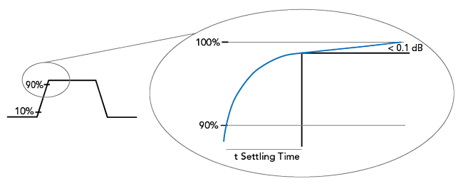
Figure 2 Pulse settling time, defined as the time for the signal to reach < 0.1 dB of its maximum value from 90 percent of the maximum. The response time is the rise time + settling time.
Without taking note of a signal’s settling time, interference can occur with the leading portion of data. Used as merit for quality control, block error rate (BLER) is the ratio between erroneous data blocks to the total blocks transmitted. Invalid data caused by settling time can lead to a high BLER, which often necessitates retransmissions and ultimately reduces network performance. Test instrumentation complemented by vendor-supplied or customer-developed power measurement software can help pinpoint the exact settling time of switching components. Software tools, for example, may enable users to place vertical and horizontal markers along the waveform. Engineers can then easily define the exact settling time window of a signal to maximize data transfer.
PROPAGATION DELAY AND WAVEFORM ANOMALIES
Ideally, TDD switches rapidly change between transmit/receive operations without a loss of data. However, some switches, especially those alternating from a power amplifier (PA) to a low noise amplifier (LNA), may experience propagation delay due to several factors, including excessive cable length, board runs, improper time adjustments or software commands.
Propagation delay is the round-trip time interval of a signal traveling from the sender, through all the necessary circuitry and networking infrastructure, to the receiving device. Even the slightest discrepancy in TDD timing from factors like propagation delay can cause serious issues, such as downlink/uplink overlap, interference and a deterioration of network performance (see Figure 3). Furthermore, the effects of propagation delay are compounded at higher mmWave frequencies with compressed switching time intervals. Any degradation in timing precision and switch performance becomes critical.
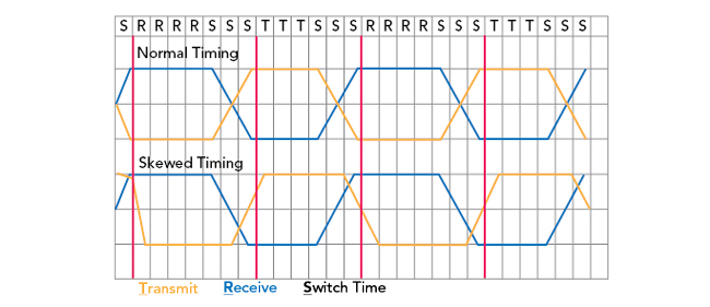
Figure 3 Normal vs. skewed timing that overlaps the transmit (yellow) and receive (blue).
Delay can also create bleed through from the PA to the LNA, leading to unwanted signal phenomena such as overshoot, which occurs when a signal exceeds its top amplitude and is often followed by ringing artifacts until the signal reaches its steady, final value. While overshoot exceeds a signal’s target, a similar effect known as undershoot occurs when a value dips below the set minimum. To maintain efficient network operation, designers must have the capability to capture and quantify the occurrence of any delay or unwanted signal phenomena in TDD circuitry.
Power sensors are key test and measurement tools to measure propagation delay and capture any signal distortion. While analyzing system performance in a test setup, measurement markers in accompanying software can pinpoint the delay window between input and output signals. Top-end sensor technology uses efficient and powerful digital signal processing techniques that eliminate gaps in acquisition and measurement latency to obtain lightning-fast performance. Fast measurement rates (e.g., 100,000 measurements per second) are made possible by capturing and processing waveform samples nearly simultaneously as opposed to serially, which avoids computational overhead, buffer size limitations and the need to stop signal acquisition.
For comparison, standard processing techniques capture waveform samples (typically during sub-1 second time intervals) and then halt acquisition for sequential data processing and transfer. Signal interference, distortion and other important events can occur during these acquisition gaps, heightening the importance of using sensors that reduce the total cycle time for acquiring and processing measurement samples. When coupled with compatible software applications, engineers can achieve real-time, gap-free acquisition of TDD signals to validate switching performance and reveal any anomalous events along the communications pathway.
SYNCHRONIZED MULTI-CHANNEL MEASUREMENTS
A situation with a single transmitter and receiver provides a simplistic TDD overview, but in more complex, practical situations there are various signals traveling at once emanating from multiple antennas, such as MIMO applications that increase radio link capacity. In this scenario, key questions arise: Are antennas switching at the same time? What is the time discrepancy between transmissions? One method to monitor more sophisticated systems is to use a vector network analyzer (VNA); however, this test instrument comes with a high price tag.
Sensors with the ability to synchronize in a test setup provide an economical alternative to a VNA, while still offering a means to monitor timing, integrity and accrued delay of numerous TDD signals. Time-aligned measurements can be achieved by using sensors that share a common time base on multiple synchronous or asynchronous channels. With this technique, the shared time base is distributed via a cable connection between the multi-function input-output ports of each sensor.
Since switching components may experience very small timing offsets, it is important to consider a test instrument’s time resolution capabilities, especially when trying to resolve a 1 to 2 ns difference in timing between TDD switches. Conventional instrumentation with standard time resolution can easily miss vital nuances between TDD signals. Currently, the finest time resolution in power measurement instrumentation is 100 ps, which not only ensures the capture of meaningful TDD waveform data, but also increases trigger stability.
While leading-edge sensors that provide synchronized multi-channel TDD measurements minimize testing costs compared to VNAs, some also provide an additional advantage of using a client’s actual signals during TDD transmission testing. Providing a simple methodology for signal optimization, clients can pinpoint delay and necessary corrections as their signals travel through TDD switches, many of which are embedded in the hardware of the RF cards. Software adjustments can then be used to fine-tune and optimize performance.
ADVANCED TEST SOLUTIONS FOR 5G TDD NETWORKS
Timing and switch performance are critical in 5G TDD network applications, especially at higher mmWave frequencies. Advanced test solutions can measure any delay experienced at various points along a 5G TDD communications path, catch signal phenomena like undershoot/overshoot, capture time between switch actuation and aid with multi-signal channel measurements. These testing solutions are enabled by key sensor capabilities such as fast rise times (3 nanoseconds), rapid measurement speed (100,000 measurements per second), wide video bandwidth (195 MHz), test setup synchronization and superior time resolution (100 ps). By choosing best-in-class test equipment, such as Boonton RTP5000 Real-Time RF Peak Power Sensors, engineers can fully capitalize on the capacity and coverage benefits of 5G TDD communications systems.