
Integrated voltage-controlled capacitors, usually known as varactors, are used in many electronic integrated devices for RF applications.1 In particular, voltage-controlled oscillators (VCO)2,3and tuneable filters4 are the two main applications. For good performance of integrated devices that have a varactor as a component, it is very important to know, a priori, the main varactor parameters. Currently, there are expressions to estimate the capacitance of a varactor; however, the problem of how to estimate its undesired resistance still remains open. There seems to be no simulation tool available that accurately computes the varactor resistance. Therefore, the designer is often forced to use first-order approximations based on empirical expressions that require previous measurements.
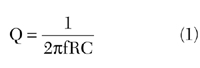
The resistance has a direct influence in the Q factor of a varactor. It is well known that the Q factor is a figure of merit usually employed to describe the performance of reactive devices. In the case of a varactor, the Q factor is defined as the ratio between the imaginary and real part of its impedance.5 In most practical cases, Equation 1 is used for its calculation.
where
R = varactor resistance
C = varactor capacitance
f = frequency
At frequencies above 2 GHz (like in WLAN, UMTS and Bluetooth), the varactor Q factor is a critical design parameter.6 For instance, its resistance determines the passive tank circuit quality of the VCO7 and consequently its phase noise. Therefore, an accurate prediction of the varactor resistance should be very important for an RF design.
There are several architectures for integrated varactors. The most common are PN junction,8 MOS9 and gated varactors.10 PN junction varactors present some advantages when compared to the others. For example, they have a better Q factor, they are easier to fabricate, and their scalability and capacitance variation is less abrupt than in MOS varactors.11
The simulation tool presented in this article has been designed for the estimation of resistance and capacitance of PN junction varactors. With this software, an RF designer will achieve an accurate varactor design, which will allow him to make reliable simulations of the circuit in which the varactor is integrated.
PN Junction Varactors
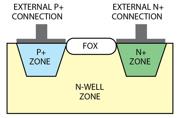
PN junction varactors are based on the variation of the PN depletion capacitance when the reverse bias voltage is varied.12 Figure 1 shows a PN junction varactor with an N-well zone with P+ and N+ contact islands. The PN junction produces the capacitance variation with reverse bias voltage. The external connections are located in N+ and P+ zones, in order to decrease the series resistance of the device. Between N+ and P+ exists a field oxide (FOX) layer to isolate the connections.13
The variation of the capacitance in the varactor is similar to the one encountered in the depletion zone of a PN junction. The value of this capacitance is given as7
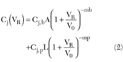
where
Cj = total capacitance (pF)
VR = reverse bias voltage (V)
Cj,b = capacitance per bottom plate area at zero voltage (pF/µm2
A = bottom plate area for P+ (µm2)
Cj,p = capacitance per side wall length at zero voltage (pF/µm)
L = total sidewall length for P+ (µm)
V0 = junction built-in voltage (V)
mb = exponent related to the bottom plate
mp = exponent related to the side walls
Programming Approximation
The way to predict the varactor resistance is based on the electromagnetic characteristics of the materials and on finite difference approximation (FDA).14 The computation and graphic representation have been implemented in the JAVA programming language.
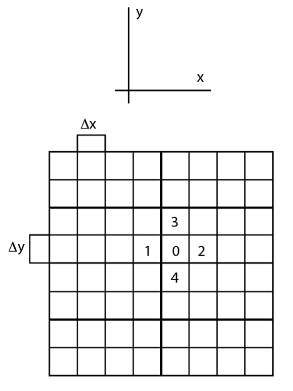
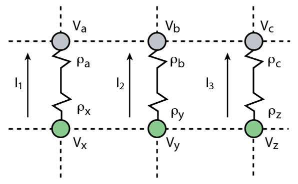
The continuous problem is transformed into a discrete one by partitioning the material surface into a grid of cells. From the given resistivity characteristics of the material, each cell is associated with its corresponding resististivity at the center of the cell (node). The next step is to calculate the voltage in each cell. It is first assumed that the material is homogeneous, that is, all the cells have the same resistivity. Figure 2 shows the discretization for a two-dimensional grid. Only five cells have been numbered, in order to show how to estimate the voltage value at the center cell (numbered 0) from the corresponding voltage values of its adjacent cells.
The estimation of this voltage is obtained using a FDA of the first and second derivatives of the voltage, that is, by the following Equations:15
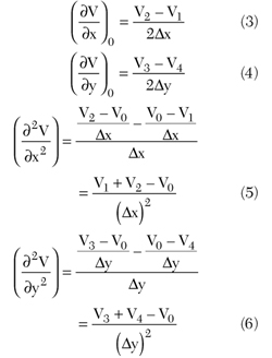
where
Vi = value of voltage in each point of the grid
 x, y = sizes of the grid cells
If the cells are square, then x = y = . From the above expressions, it is possible to approximate the Laplace expression for the continuous problem as15
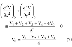
The size of the cell determines the accuracy. Notice that this expression can only be used for homogeneous materials. The discrete area to study is initialised by points with known voltage. Therefore, the first iteration begins by knowing the voltages at the cells located at the boundary (applied voltage in the external connections). By using Equation 7 the voltage of a cell node is calculated from the adjacent cells.
In each iteration, the new voltage values are computed based on the previously computed voltages. The process finishes when the error between iterations is less than a predetermined error coefficient.16 At that time, the grid voltage values are accepted as the actual voltage distribution along the surface. To minimize the error, it is useful to modify the direction of the rack in each iteration.17 Usually, the process converges in four iterations.
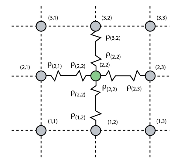
If the material is not homogeneous the algorithm must be modified to include the resistivity variations on each cell. Referring to Figure 3 , the voltage estimation is then computed as7
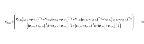
where
 i,i= resistivity in each cell
Vi,i = voltage value in each cell
Once the voltage matrix grid has been obtained, the next step is to estimate the current that flows through the varactor surface. This can easily be computed by using the voltage and resistivity matrix grid.
Figure 4 shows the method used to calculate the current. The dotted node of the center cell belongs to the contact of the varactor and has a fixed voltage. The adjacent node cells have the previously calculated voltages. The current flows from the central node to the four adjacent nodes, and is simply given by
After calculating all currents and voltages, the varactor resistance can be obtained from Ohm's law as
Finally, the estimation of the varactor capacitance is based on a modification of Equation 2, that gives more accurate values.
Software Tool
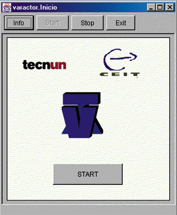
The developed tool has been named "Varactool." The main window of this simulation tool is shown in Figure 5 . The aim of the application is to give the designer an easy way to introduce the parameters corresponding to the fabrication technology used, and the geometric parameters of the varactor. Technology parameter values can be modified through the console, and it is possible to calculate the effect they have on capacitance and resistance.
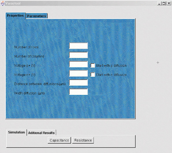
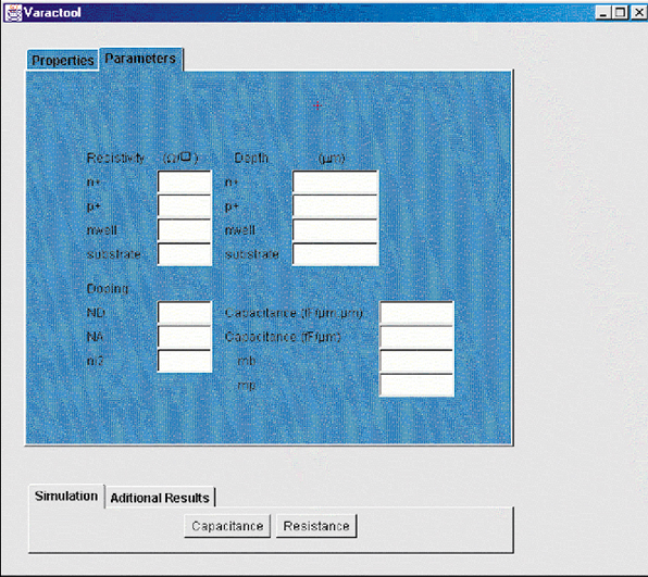
Before calculating resistance and capacitance, the designer must introduce the technology parameters in the next window (Figure 6 ). Design values are typed in this window. The geometric parameters of the varactor are entered in the next window (Figure 7 ).
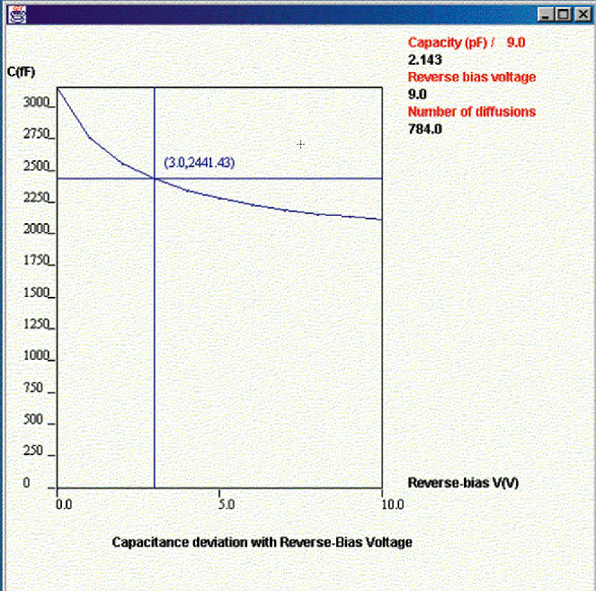
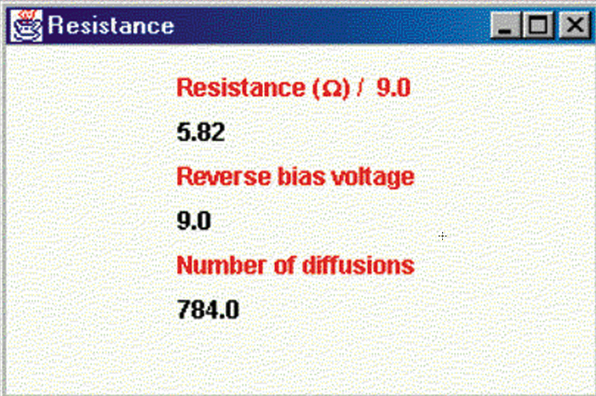
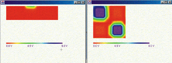
The estimation of the capacitance is shown in Figure 8 . This graphic representation of the results also shows the variation of the capacitance versus reverse voltage. By dragging the mouse, the capacitance versus voltage can be displayed. Figure 9 shows the window with the resistance value. Other additional results such as voltage variation along the surface area and the vertical cross-section can also be shown, as seen in Figure 10 .
Experimental Results
In order to verify the results obtained with Varactool, two PN junction varactors were simulated and their parameters estimated with this software tool. Later, these varactors were fabricated and their actual measurements were compared with the estimated results. The fabrication technology used was an Austriamicrosystem (AMS) SiGe 0.8 µm standard process. The geometrical characteristics of the varactors are shown in Table 1 .
|
Table 1 | ||
|
|
Varactor 1 |
Varactor 2 |
|
Number of square diffusion areas |
(28 x 28) |
(28 x 56) |
|
Distance between diffusions (µm) |
2 |
2 |
|
Diffusions width (µm) |
2 |
2 |
|
Table 2 | |||
|
|
Measured |
Simulated |
Error |
|
Varactor 1 |
5.98 |
5.82 |
2.6 |
|
Varactor 2 |
9.46 |
9.33 |
1.3 |
 )
) 
The two varactors were measured over a 0 to 9 V biasing range, applied to the N+ terminal with the P+ terminal connected to ground. The measurement system used for the characterization of the varactors consists of the HP8719ES vector network analyzer and Cascade ACP40 GSG microprobes. To calibrate the measuring system, the short-open-load-through (SOLT) method was used. Finally, a four-step de-embedding method18was used to remove the parasitic effects introduced by the measurement structures. Table 2 compares the measured resistance for each varactor with the one estimated with Varactool.
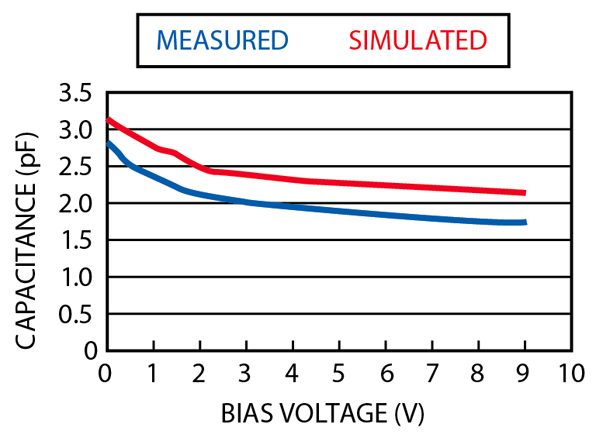
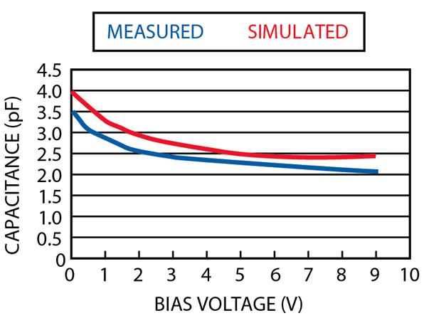
The measured results of capacitance of Varactor 1 are compared with the simulations for different bias voltages in Figure 11 . From the values shown, the estimated error between the measured and simulated capacitance of Varactor 1 is around 15 percent. The measured results of the capacitance of Varactor 2 are compared with the estimated results for different bias voltages in Figure 12 . From the values shown, the average error between the measured and estimated capacitance of Varactor 2 is approximately 14 percent.
Conclusion
A varactor simulation tool called "Varactool," based on the finite difference approximation, has been developed. It allows the prediction of both capacitance and resistance of PN junction varactors, using a friendly interface and a convenient graphic representation of the results. Two PN junction varactors have been fabricated using AMS SiGe 0.8 µm technology. Their resistance and capacitance have been measured. The error between Varactool predictions and measurements is less than three percent in resistance, and less than 19 percent in capacitance (over the tuning range). The simulated resistance given by Varactool may be used in the calculation of the Q factor in an IC for RF applications. Since accurate values for resistance and capacitance can be obtained with the Varactool tool, the estimation of Q factors will also be accurate. It should be mentioned that the simulated capacitance values are larger than the measured ones. The main reason is that Varactool does not take into account the external connexions. Finally, since this simulation tool allows different varactor geometries, it gives to the RF designer the flexibility to choose the most adequate varactor design for each device.
The Varactool program can be downloaded from the Web at www.ceit.es/rf/index.htm.
References
1. M. Steyaert, M. Borremans, J. Janssens and B. De Muer, "RF Communication Circuits," The VLSI Handbook , CRC Press & IEEE Press, 1999.
2. P. Andreani and S. Mattisson, "A 2.4 GHz CMOS Monolithic VCO Based on an MOS Varactor," Proceedings of the 1999 International Symposium on Circuits and Systems, May-June 1999.
3. E. Hern‡ndez, "Fully Integrated CMOS VCO for UMTS Direct Conversion Receivers," Applied Microwave and Wireless , Vol. 14, No. 9, September 2002.
4. U. Karacaoglu and D. Robertson, "DIC Active Bandpass Filters Using Varactor-tuned Negative Resistance Differences," IEEE Transactions on Microwave Theory and Techniques , Vol. 43, No. 12, December 1995.
5. K.B. Ashby, "High Q Inductors for Wireless Applications in a Complementary Silicon Bipolar Process," IEEE Journal of Solid-State Circuits , Vol. 31, No. 6, June 1996.
6. U.L. Rohde and D.P. Newkirk, RF/Microwave Circuit Design for Wireless Applications , Wiley-Interscience, 2000.
7. J. Aguilera, "Inductores Integrados de Alto Factor de Calidad en una Tecnología Est‡ndar 0.8 mm SiGe," PhD Thesis, TECNUN (Universidad de Navarra), March 2002.
8. A.S. Porret, T. Melly, C.C. Enz and E.A. Vittoz, "Design of High Q Varactors for Low Power Wireless Applications Using a Standard CMOS Process," IEEE Journal of Solid-State Circuits , Vol. 35, No. 3, March 2000, pp. 337-345.
9. F. Svelto, P. Erratico, S. Manzini and R. Castello, "A Metal-oxide-semiconductor Varactor," IEEE Electron Device Letters , Vol. 20, No. 4, April 1999, p. 164.
10. W.M.Y. Wong, P.S. Hui, Z. Chen, K. Shen, J. Lau, P.C.H. Chan and P.K. Ko, "A Wide Tuning Range Gated Varactor," IEEE Journal of Solid-State Circuits , Vol. 35, No. 5, May 2000, pp. 773-779.
11. E. Pedersen, "RF CMOS Varactors for Wireless Applications," PhD Thesis, RISC Group, Alborg University, Denmark.
12. R. Pierret, Fundamentos de Semiconductores , Addison-Wesley Iberoamericana, 1995.
13. R.J. Baker, H.W. Li and D.E. Boyce, "CMOS Circuit Design, Layout and Simulation," IEEE Press Series on Microelectronics Systems, 1998.
14. C.M. Bender and S.A. Orszag, Advanced Mathematical Methods for Scientists and Engineers , McGraw Hill, College Division, 1978.
15. R.A. Decarlo and P. Lin, "Linear Circuit Analysis: Time Domain, Phasor and Laplace Transform Approaches," The Oxford series in Electrical and Computer Engineering, February 2001.
16. J. Jin, The Finite Difference Method in Electromagnetics , Wiley-Interscience, 1993.
17. M.W. Bern, J.E. Flahertly and M. Luskin, "Grid Generation and Adaptive Algorithms," Springer Verlag, Berlin, 1999.
18. T.E. Kolding, "On Wafer Calibration Techniques for Gigaherz CMOS Measurements," Proceedings of IEEE International Conference on Microelectronic Test Structures (ICMTS), March 1999.
 Nekane Sainz is a PhD candidate in telecommunication engineering. Her research interests include passive RF components and the use of simulation tools for designing. She is currently working on passive tuneable filter design.
 Iñigo Gutierrez received his degree in industrial engineering and is a PhD candidate. His research focuses on the design and characterization of passive elements for RF applications. He is currently working on RF integrated varactor design.
 Armando Muñoz worked for six years as an R&D engineer, R&D manager and RF division director at Fagor Electr-nica S.C.I. He was involved in tuners and RF subassemblies design and manufacturing. In 1979, he joined IKUSI, SA, as technical director, and, from 1985 to 2000, was general manager of the RF division. During his stay at IKUSI, he led several projects in the areas of optical communications, CATV, radio frequency, microwaves, radio control and DTV. Since 2000, he has worked at TECNUN, University of Navarra.
 Joaquín de Nó is a researcher and assistant director of the electrical, electronic and control engineering department of the school of engineering, TECNUN, of the University of Navarra, San Sebastian, Spain. de Nó received his PhD in 1996, after having worked on the development and application of simulation tools for the resolution of electric and electronic problems. At present, his research is focused on the integration of passive devices for RF applications. He has participated in four industrial projects and is author or co-author of six technical papers.
 Erik Hernández received his BS and MS degrees in electronic engineering from ESI of the University of Navarra in 1999, and then joined TECNUN's RF integrated circuit design group, San Sebastian, Spain. He obtained his PhD degree in monolithic voltage-controlled oscillators for RF applications in December, 2002. His main interests include the design and characterization of passive components and mixers in standard low cost technologies.
 Andrés García-Alonso received his PhD in 1993. He is currently the director of the electronics and communications department of CEIT. Between 1996-97, he worked at the Fraunhofer Institut fŸr Integrierte Schaltungen, Erlangen, Germany. His research is focused on the design of analog integrated circuits for communication front ends. He has taken part in 11 industrial projects, being the manager of four others. He is author or co-author of 30 technical publications.