

5G wireless systems and connected devices are proliferating across every imaginable industry, driving technology leaders to capitalize on market opportunities for RF-enabled products defined and differentiated by performance, size and cost. Traditionally, custom or proprietary integrated circuit (IC) designs leveraging the latest advanced technology node have been the path forward to realize differentiation, but today’s complex designs are moving beyond the chip.
RF and mixed-signal engineering efforts have embraced not only diverse semiconductor processes but advanced cross-fabric packaging and system-in-package (SiP) and package-in-package (PiP) technologies, as well as 3D ICs implemented using advanced interconnect technologies. Successful products require every possible component interaction which might influence the overall performance of the final product be considered at the system level throughout the design, analysis and signoff phases of development. All electrical factors affecting the outcome—micro and macroscopic—must be considered.
To win in the highly competitive 5G wireless markets, companies require electronic design automation (EDA) solutions enabling complete and comprehensive RF workflows from the chip to the system. To this point, engineering teams and EDA platforms, as well as simulation and analysis technologies, have converged to ensure valuable engineering time is spent designing—not transferring and translating data from one tool to another. EDA software developers must provide an efficient front to back end interoperable workflow to maximize user productivity.
With the Cadence acquisition of AWR® from National Instruments in 2020, the latest V16 release of the Cadence® AWR Design Environment® platform offers complete and comprehensive RF workflows (see Figure 1).
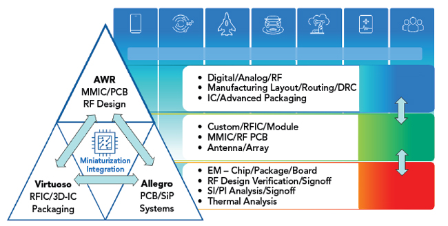
Figure 1 The Cadence RF EDA solution provides a comprehensive design workflow.
HETEROGENEOUS TECHNOLOGIES
Heterogeneous integration mitigates the high cost of homogeneous system-on-chip (SoC) solutions by enabling designers to combine proven RFIC and MMIC designs on substrates using newer packaging technologies. Advanced integration methods such as fan-out wafer-level packaging can result in smaller and more efficient systems, yet these highly integrated systems are more complicated and prone to error from the interdependencies of the individual components, the complex network of cross-fabric interconnects and the challenges of assembling cross-platform design data from multiple sources. Platform interoperability is crucial for multi-technology integration across chip, package and board design (see Figure 2).
Figure 2 The AWR software platform supports IC to system design.
The new V16 release of AWR Design Environment enables at least a 50 percent reduction in turnaround time through workflow automation. It achieves this by leveraging RF intellectual property (IP) creation and cross-platform simulation, including the IC and package (Virtuoso flow) and the board (Allegro flow). Additionally, integration and interoperability of the Clarity™ 3D Solver and Celsius® Thermal Solver provide electrothermal co-simulation and coupled analyses of large, densely populated designs such as RF front-ends. The RF workflow innovations enabled by the V16 release start with a foundational advance in the way design data and software IP are shared and transferred across manufacturing-specific design platforms. Under the Cadence umbrella, the level of RF integration being introduced with V16 software significantly improves engineering team productivity.
Cadence platforms have continually evolved to address the manufacturing, design and analysis requirements of the process technologies they support, with the design flow automation to manage the development of extremely complex chip, package and board systems. As system-level integration calls for RF design across these different technologies, prior to starting the design, engineers are pulling information from multiple sources: business requirements, reliability constraints, manufacturing processes and supply chain data. For enterprises and large design teams, the need to efficiently share libraries and work with company-authorized and pre-approved component parts and material stackups adds to the challenge of getting a product to market quickly. Interoperability between platforms is necessary to share design data and leverage the unique features of the different tools and reduce or eliminate system integration bottlenecks. Any disconnect between the RF design and manufacturing layout teams consumes engineering resources and directly impacts development schedules.
Imagine RF IP created within AWR software seamlessly integrated into systems designed with newer process technologies and integration methodologies. Development teams now have a highly efficient RF workflow enabling them to extract AWR RF IP/design data and reuse it in the appropriate RFIC, PCB or SiP platform. The V16 release introduces this support for Cadence unified libraries and technology files, establishing interoperability between the AWR, Virtuoso and Allegro platforms.
VIRTUOSO & AWR WORKFLOW
Leveraging a shared architecture and data across the Cadence EDA solutions, the V16 release provides for new RF workflows taking completed designs from Microwave Office software and passing both the schematic and layout to the Virtuoso and/or Allegro platforms. The data is in a unified library and contains all the building blocks of the circuit design. This enables design teams to operate the Allegro SiP or Virtuoso SiP bidirectional implementation flow and Virtuoso RF Solution physical implementation flow as the primary layout tool, with V16 software providing the RF IP schematic and layout design data. The Virtuoso RF Solution flow captures Microwave Office RF IP, enabling designers to represent, integrate and verify the MMIC and embedded RF package design within a single environment. The shared database enables more practical package and IC co-design by simplifying the design flow with easy and reliable access to RF IP developed within Microwave Office.
For example, Microwave Office users can design passive off-chip components through circuit design, optimization and EM verification and then decide the best implementation technology. In some cases, a network of passive components may best be implemented across the IC package boundary. This is often true for RF modules, where the ideal filter design, matching networks and power amplifier output stage load termination use components on both the die and the package substrate.
Within the Virtuoso RF Solution environment, the Spectre® Simulation Platform engine can simulate Microwave Office linear models to support IC and module co-design with embedded Microwave Office IP. The ability to import this IP into the Virtuoso flow extends to MMIC designs. Since most MMIC model and PCell libraries are defined and implemented by the III-V foundry as a process design kit (PDK), the Microwave Office MMIC design flow uses this PDK for the target semiconductor process in the design. The resulting MMIC schematic and layout can then be exported as a unified library design and imported into the Virtuoso environment (see Figure 3).
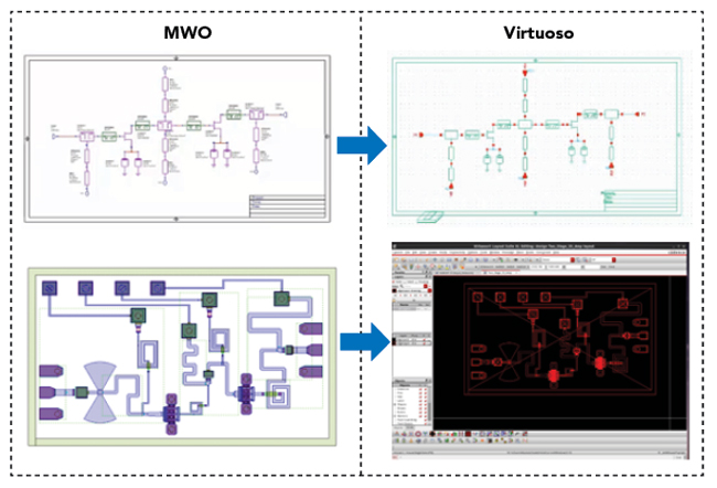
Figure 3 A two-stage MMIC amplifier design imported from AWR into Virtuoso.