
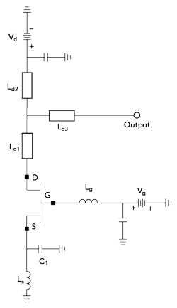
Figure 1 Colpitts oscillator.
Two MMIC oscillators at 28 and 38 GHz, respectively, were fabricated with a 0.15 µm GaAs enhancement-mode (E-mode) PHEMT process using a Colpitts topology modified for high frequency performance. For higher output power and better efficiency, a T-shaped network on the load side was optimized for output matching. The 28 GHz oscillator delivered an output power of 16.7 dBm with a DC-to-RF efficiency of 24.3 percent, while the 38 GHz oscillator delivered an output power of 10.6 dBm with a DC-to-RF efficiency of 10.3 percent. Measured phase noise at 1 MHz offset was -115.8 dBc/Hz at 28 GHz and -110.4 dBc/Hz at 38 GHz.
mmWave frequency sources with low phase noise, low-power dissipation and sufficient output power are essential elements of wireless communication systems. Because heterojunction bipolar transistors (HBTs) exhibit lower device 1/f noise compared with high electron mobility transistors (HEMTs), they are often used for low phase noise oscillators.1 Many results have been reported for Ka- and K-Band oscillators fabricated with GaAs or SiGe HBTs,2,3 however, these oscillators have either high DC power consumption or insufficient output power. HEMTs can deliver greater power at higher oscillating frequencies,4 with several Ka-Band HEMT MMIC oscillators reported.5-7 The E-mode PHEMT is suitable for modern wireless communications due to its single supply voltage and low knee voltage.8
In this article, we discuss the design and performance of two Ka-Band oscillators designed on the same 0.15 µm GaAs E-mode PHEMT process. High DC-to-RF efficiency and low phase noise were obtained. To achieve high oscillating frequency, a modified Colpitts topology was adopted and a T-shaped output matching network was used to achieve higher output power and efficiency. With this approach, oscillators at 28 and 38 GHz delivered 16.7 and 10.6 dBm output power and high DC-to-RF efficiencies of 24.3 and 10.3 percent, respectively. The modified Colpitts topology enables a low gate voltage bias without influencing oscillation start-up. This results in lower gate shot and 1/f noise, reducing their contributions to the oscillator’s phase noise. The measured phase noise at 1 MHz offset was -115.8 dBc/Hz at 28 GHz and -110.4 dBc/Hz at 38 GHz.
MMIC PROCESS AND CIRCUIT DESIGN
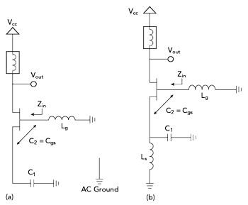
Figure 2 Traditional low frequency Colpitts design (a), modified for better high frequency performance (b).
The circuit design was based on the 0.15 µm GaAs E-mode PHEMT devices on a process offered by WIN Semiconductors Corporation. The E-mode PHEMT device typically exhibits a maximum oscillation frequency, fmax, of 150 GHz and a current gain cutoff frequency, fT, of 80 GHz when biased for maximum DC transconductance of ~1,000 mS/mm. The threshold voltage for the devices is ~0.25 V. The MMIC process includes slot vias, thin film resistors, metal-insulator-metal (MIM) capacitors, spiral inductors and microstrip transmission lines.
A Colpitts topology was used for the oscillator (see Figure 1). The inductive elements Lg and Ls were achieved using short microstrip lines less than λ/4 and the capacitance, C1, was realized with an open microstrip line or MIM capacitor. For a traditional lower frequency Colpitts oscillator (see Figure 2a), the resonator is typically formed by C1 and Lg. For the high frequency oscillators described here, an additional inductance, Ls, was introduced to improve performance (see Figure 2b). In this design, the internal gate-source capacitance of the transistor, Cgs, serves as C2.
Using an ideal transconductance model, the circuits were analyzed under small-signal conditions to understand the effect of Ls (see Figure 3). The input impedance of the model in Figure 3a is
where the negative real part of Zin corresponds to the negative resistance. The value of negative resistance is smaller at higher frequencies. From Figure 3b,
In the mmWave band, 4π2f 2C1C2 > 4π2f 2C1C2 – C2/Ls > 0. With Ls included, the negative resistance is boosted at higher frequencies, which improves oscillation start-up and enables higher efficiency. From Equations 1 and 2, the imaginary part of Zin is a capacitive reactance. To create oscillation, an externally connected inductive component at the gate terminal, Lg, pairs with the opposite reactance of the PHEMT device.
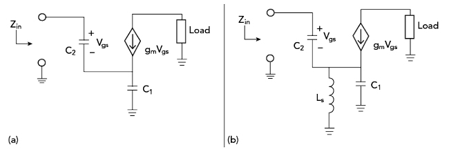
Figure 3 Small-signal models of the low frequency (a) and high frequency (b) designs.
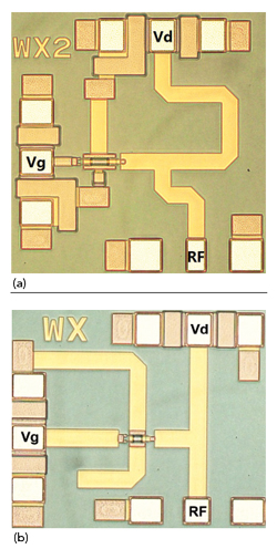
Figure 4 28 GHz (a) and 38 GHz (b) oscillator MMICs.
The HEMT device cells had 2 x 100 μm and 2 x 50 μm gate widths at 28 and 38 GHz, respectively, and were biased at Vds = 4 V and Vgs = 0.45 V. Since the added Ls enhances the negative resistance, the transistor can be biased at a lower gate voltage and drain-source current without inhibiting the conditions for oscillation. This enhances efficiency and reduces the gate shot and 1/f noise, achieving lower oscillator phase noise.9
The load design was optimized for higher output power and better DC-to-RF efficiency. Theoretically, maximum output power is realized with complete reactive compensation, so an inductive load was employed to compensate the capacitive device output reactance. A λ/4 transmission line was not used as the RF choke in the supply path; instead, the microstrip line Ld2, shorter than λ/4, was employed as the inductive element (see Figure 1). The T-shaped network Ld1-d3 serves as output matching at the load side to achieve better power and efficiency. In this way, the circuit structure was simplified since the matching lines also provide the bias.
The circuit was simulated using Keysight’s Advanced Design System, first using small-signal analysis to determine the oscillating frequency. Then, harmonic balance and transient analyses were performed to determine the output power. Finally, the layout was simulated and optimized using the Momentum 2.5D planar electromagnetic simulator. The harmonic balance simulation predicted the 28 GHz oscillator would achieve an output power of 17.9 dBm with an efficiency of 29 percent, and the 38 GHz oscillator would achieve an output power of 12.4 dBm with an efficiency of 17 percent.
EXPERIMENTAL RESULTS
The two MMICs are shown in Figure 4. The 28 and 38 GHz MMIC sizes are 750 μm x 760 μm and 740 μm x 640 μm, respectively, including the DC and RF probe pads.
The E-mode PHEMT oscillator MMICs were fully characterized on-wafer at room temperature using a Keysight N9030A PXA signal analyzer. Measuring the 28 GHz oscillator, a 6 dB attenuator was added to protect the analyzer from high output power. For the 38 GHz measurement, the attenuator was not needed. The cables and probes had 3.3 dB loss at 28 GHz and 3 dB loss at 38 GHz; the two MMICs were measured with different cables, which is why the cable loss at 38 GHz is lower. Accordingly, the measured output power values at 28 and 38 GHz were corrected by 9.3 and 3 dB, respectively, to account for the loss of the attenuator, probes and cables.
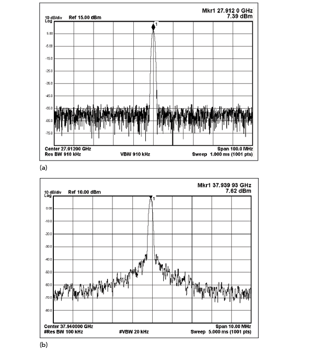
Figure 5 Measured spectrum of the 28 GHz (a) and 38 GHz (b) oscillators.
Figure 5 shows the measured spectrum of the two oscillators into a standard 50 Ω load. For the 28 GHz oscillator, an uncalibrated output power of 7.4 dBm corresponded to an actual output power of 16.7 dBm, compensating for the attenuator, cable and probe losses. For the 38 GHz oscillator, an uncalibrated output power of 7.6 dBm corresponded to an actual value of 10.6 dBm. With dissipated powers of 192 and 112 mW, respectively, the DC-to-RF efficiencies were 24.3 and 10.3 percent. The measured phase noise was -115.8 dBc/Hz at 1 MHz for the 28 GHz oscillator and -110.4 dBc/Hz at 1 MHz for the 38 GHz design (see Figure 6).
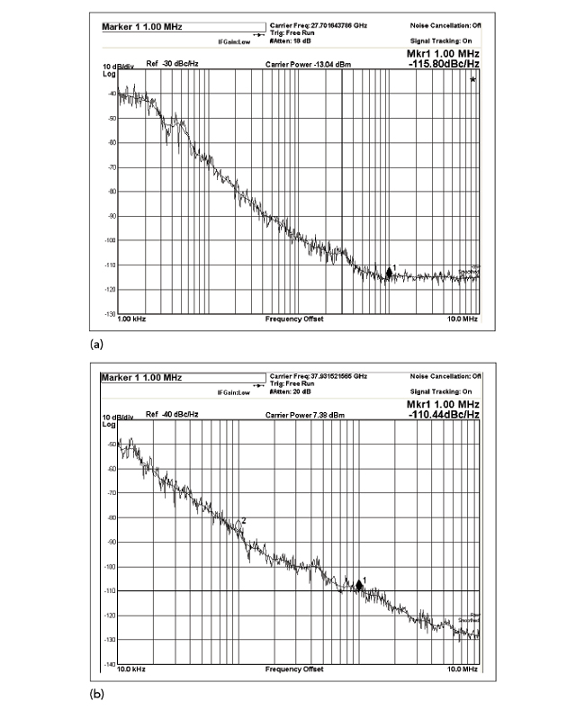
Figure 6 Measured phase noise of the 28 GHz (a) and 38 GHz (b) oscillators.
Generally, an oscillator's performance is evaluated by the figure of merit, FOM:10
where L(Δf) is the phase noise at offset frequency Δf, f0 is the oscillation frequency and P is the power dissipation. The calculated FOMs of the 28 GHz and 38 GHz oscillators at 1 MHz are -181.9 dBc/Hz and -181.7 dBc/Hz, respectively.
SUMMARY
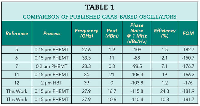
mmWave MMIC oscillators at 28 and 38 GHz were developed using a 0.15 μm GaAs E-mode PHEMT process. The oscillators demonstrated excellent efficiency and phase noise performance with sufficient RF output power to drive a mixer without a buffer amplifier. DC-to-RF efficiency and phase noise performance was state-of-the-art for GaAs-based oscillators operating at this frequency. The performance of several published free-running GaAs-based oscillators is compared with these designs in Table 1. This work demonstrates the potential of GaAs E-mode PHEMT technology for high performance mmWave sources in wireless communication systems.
Acknowledgment
This project was supported by the National Natural Science Foundation of China (Grant No. 61434006).
References
- Q. Zou, K. Ma and K. S. Yeo, “A Low Phase Noise and Wide Tuning Range Millimeter-Wave VCO Using Switchable Coupled VCO-Cores,” IEEE Transactions on Circuits and Systems I: Regular Papers, Vol. 62, No. 2, February 2015, pp. 554–563.
- F. Padovan, M. Tiebout, K. L. R. Mertens, A. Bevilacqua and A. Neviani, “Design of Low-Noise K-Band SiGe Bipolar VCOs: Theory and Implementation,” IEEE Transactions on Circuits and Systems I: Regular Papers, Vol. 62, No. 2, February 2015, pp. 607–615.
- A. Kurdoghlian, M. Sokolich, M. Case, Miro Micovic, S. Thomas III and C.H. Fields, “38 GHz Low Phase Noise CPW Monolithic VCO’s Implemented in Manufacturable AlInAs/InGaAs HBT IC Technology,” IEEE GaAs Integrated Circuits Symposium Digest, November 2000, pp. 99–102.
- A.P.S. Khanna, “State of the Art in Microwave VCOs,” Microwave Journal, Vol. 46, No. 10, May 2015, pp. 22–42.
- W. K. Huang, Y. A. Liu, C. M. Wang, Y. M. Hsin, C. Y. Liu and T. J. Yeh, “Flip-Chip Assembled GaAs pHEMT Ka-Band Oscillator,” IEEE Microwave and Wireless Components Letters, Vol. 17, No. 1, January 2007, pp. 67–69.
- W. Lee, S. Lee, J. Choi, J. So and Y. Kwon, “Ka-Band VCO with Parasitic Capacitance Cancelling Technique,” Electronics Letters, Vol. 53, No. 1, January 2017, pp. 38–40.
- Y. Chen, K. Mouthaan and F. Lin, “Design of X-Band and Ka-Band Colpitts Oscillators Using a Parasitic Cancellation Technique,” IEEE Transactions on Circuits and Systems I: Regular Papers, Vol. 57, No. 8, August 2010, pp. 1817–1828.
- L. H. Chu, E. Y. Chang, S. H. Chen, Y. C. Lien and C. Y. Chang, “2 V-operated InGaP-AlGaAs-InGaAs Enhancement-Mode Pseudomorphic HEMT,” IEEE Electron Device Letters, Vol. 26, No. 2, February 2005, pp. 53–55.
- H.A.W Markus, “Low-Frequency Noise in Modern Semiconductor Transistors,” PhD Thesis, Eindhoven, 1997.
- H. Y. Chang, Y. S. Wu and Y. C. Wang, “A 38 Percent Tuning Bandwidth Low Phase Noise Differential Voltage Controlled Oscillator Using a 0.5 μm E/D-pHEMT Process,” IEEE Microwave and Wireless Components Letters, Vol. 19, No. 7, July 2009, pp. 467–469.
- H. Y. Chang, C. H. Lin, Y. C. Liu, W. P. Li and Y. C. Wang, “A K-Band High Efficiency High Power Monolithic GaAs Power Oscillator Using Class-E Network,” IEEE Microwave and Wireless Components Letters, Vol. 27, No. 1, January 2017, pp. 55–57.
- C. C. Chiong, H. Y. Chang and M. T. Chen, “Ka-Band Wide-Bandwidth Voltage-Controlled Oscillators in InGaP-GaAs HBT Technology,” Proceedings of the 3rd European Microwave Integrated Circuits Conference, October 2008, pp. 358–361.