
Figure 16 shows the simulated performance with C-Band operation. PAE is better than 50 percent, with output power of 34.8 dBm and associated gain of 11.8 dB. At L-Band, the PAE, output power and gain are low: 14.1 percent, 25.4 dBm and 2.9 dB, respectively.
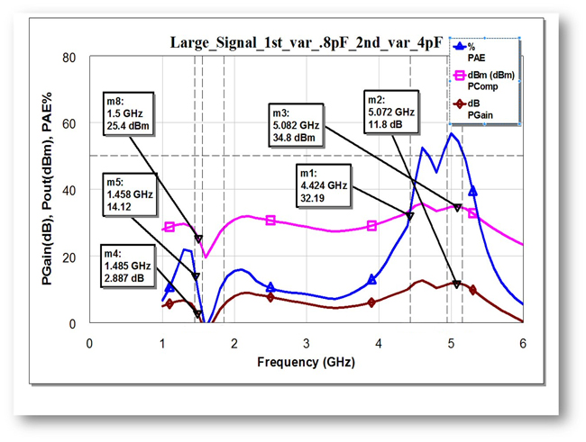
Figure 16 Large-signal simulation with C-Band selected: PAE, Pout and saturated gain vs. frequency.
To reject one of the two bands — C-Band for example (see Figure 15) — the capacitance for the second varactor is set to 4 pF, and the first varactor’s capacitance is 0.8 pF. To reject L-Band (see Figure 16), the capacitance values are flipped: the first varactor’s capacitance is set to 4 pF, the second varactor’s to 0.8 pF. Recall that the capacitance required to operate in both bands simultaneously with good gain and efficiency, i.e., concurrent dual bands, is 0.8 pF for both varactors. To reject one of the bands, the capacitance value is set to 4 pF for one of the two varactors. This requires a varactor tuning ratio of 5:1.
MEASURED vs. SIMULATION
Measured |S21| and |S11| of the BST varactors used in the reconfigurable PA board is compared with the simulated performance for two bias states: 0 and 6 V (see Figures 17–18). The varactor current was limited to 1 μA, which determined the maximum bias voltage applied: 6 V with these devices. The measured variation in capacitance agrees well with the simulated capacitance value of 2.8 pF for 0 V bias and 1.5 pF for 6 V bias, a 1.9:1 tuning ratio.
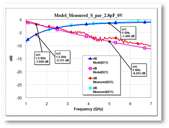
Figure 17 Measured vs. simulated |S21| and |S11| with 0 V varactor bias, an approximate capacitance of 2.8 pF.
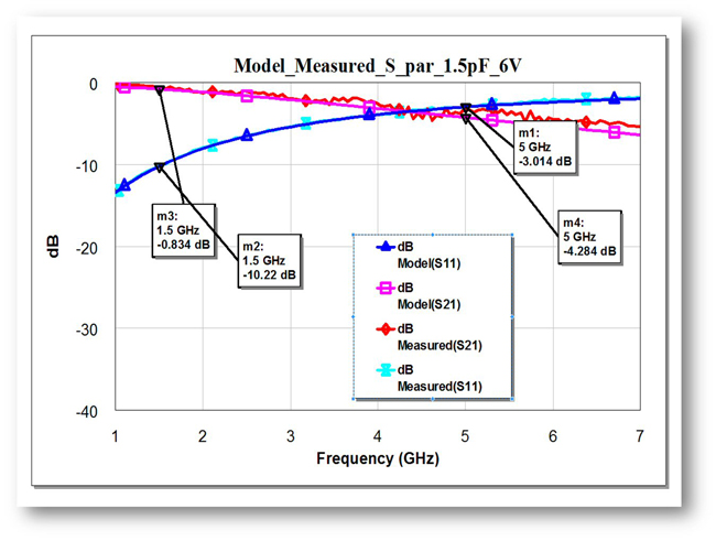
Figure 18 Measured vs. simulated |S21| and |S11| with 6 V varactor bias, an approximate capacitance of 1.5 pF.
Figure 19 compares the measured data with the small-signal simulation with both varactors biased to 1.5 pF capacitance, i.e., both varactors on. The measured gain generally matched the predictions with both varactors biased to 1.5 pF capacitance; discrepancies occurred because the varactor capacitance values did not meet the design requirements.
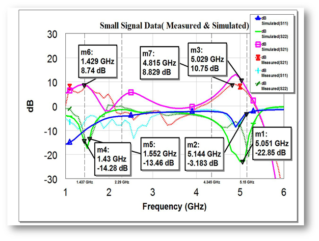
Figure 19 Measured vs. simulated small-signal performance with both varactors set to 1.5 pF.
Figure 20 shows the simulated efficiency, output power and gain with both varactors biased to 1.5 pF capacitance. To construct this plot, measured parameters matching the small-signal simulated data were used, e.g., 1.5 pF varactor capacitance, 44 mA device drain current. The PA is predicted to have a PAE of 47.4 percent, Pout of 30.7 dBm and associated gain of 7.6 dB at L-Band, and a PAE of 62.9 percent, Pout of 32.8 dBm and associated gain of 10.3 dB at C-Band.
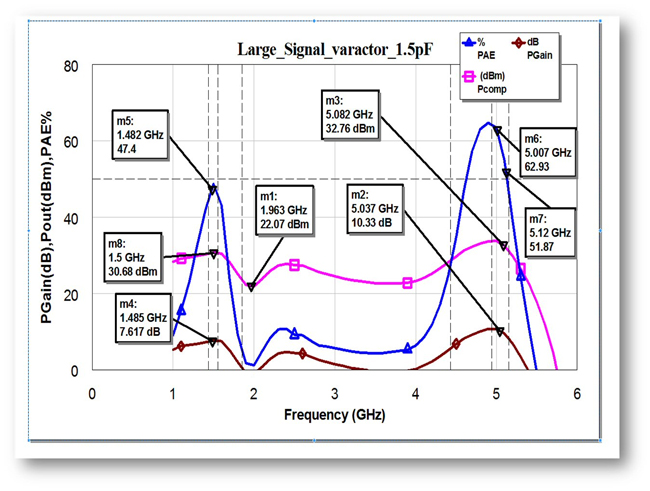
Figure 20 Simulated PAE, Pout and associated gain for the PA in dual-band mode.
CONCLUSION
This article presented the design of a reconfigurable, concurrent, dual-band PA operating at the L and C telemetry bands. Using a 0.25 μm GaN HEMT and tunable components solely in the input matching section predicts high efficiency in both bands, which makes this design unique. Small-signal measured data verifies the dual-band performance, and large-signal simulation using measured small-signal data predicts efficiency above 45 percent for L-Band and above 60 percent for C-Band with a varactor capacitance of 1.5 pF.
Better small-signal response — higher gain, better input and output return loss — and better large-signal response — higher PAE and output power — can be achieved with varactors having 5:1 capacitance tuning or with values closer to the design values of 4 pF at no bias and 0.8 pF with bias. Achieving the desired capacitance values and tuning ratios, the PA can achieve its design goals. BST varactors with higher tunability are being fabricated to verify the simulations.
To the best of the authors’ knowledge, this design represents the first high efficiency, reconfigurable, concurrent dual-band PA suitable for telemetry applications.
ACKNOWLEDGMENT
This research is supported by the Air Force Office of Scientific Research (Program Officer: Dr. Michael Kendra). We would like to thank Dr. Paul Watson, Mr. Tony Quach, Ms. Aji Mattamana, Mr. Will Gouty and Mr. Steve Dooley for their technical support and advice. The authors would also like to thank Modelithics for the transistor models used in this design, which were provided as part of Modelithics' University Program.
References
- “Part I: Telemetry Standards,” Document 106-15, Telemetry Group, Range Commanders Council, White Sands Missile Range, New Mexico, June 2015. Web. http://www.irig106.org/docs/106-15/
- U. Kim, J. -L. Woo, S. Park and Y. Kwon “A Single Chain Multiband Reconfigurable Linear Power Amplifier in SOI CMOS,” IEEE MTT-S International Microwave Symposium, May 2015.
- H. Okazaki, S. Narahashi, A. Fukuda and T. Miki, “Band Reconfigurable High-Efficiency Power Amplifier Using MEMS Switches,” IEEE International Workshop on Radio-Frequency Integration Technology: Integrated Circuits for Wideband Communication & Wireless Sensor Networks, November-December 2005, pp. 83-86.
- H. Zhang, H. Gao and G. -P. Li, “Broad-Band Power Amplifier with a Novel Tunable Output Matching Network,” IEEE Transactions on Microwave Theory and Techniques, Vol. 53, No. 11, November 2005, pp. 3606-3614.
- H. Katta, H. Kurioka and Y. Yashima “Tunable Power Amplifier Using Thin-Film BST Capacitors,” IEEE MTT-S International Microwave Symposium Digest, June 2006, pp. 564-567.
- W.C.E. Neo, Y. Lin, X. -D. Liu, L. C. N. De Vreede, L. E. Larson, M. Spirito, M. J. Pelk, K. Buisman, A. Akhnouk, A. De Graauw and L.K. Nanver, “Adaptive Multi-band Multi-Mode Power Amplifier Using Integrated Varactor-Based Tuanble Matching Networks,” IEEE Journal of Solid-State Circuits, Vol. 41, No. 9, September 2006, pp. 2166-2176.
- T. Quach et al, “Frequency-Agile and Power Scalable Power Amplifier for Multi-band Telemetry Applications,” The ITEA Journal, December 2016.
- K.Chen, X. Liu and D. Peroulis “Widely Tunable High Efficiency Power Amplifier with Ultra Narrow Instantaneous Bandwidth,” IEEE Transactions on Microwave Theory and Techniques, Vol. 60, No. 12, December 2012, pp. 3787-3797.
- U. Nath, T. Quach, A. G. Mattamana, S. Dooley, W. Gouty, P. Watson and G. Subramanyam “Concurrent Dual-Band Hybrid Power Amplifier Using 0.25 μm GaN Technology,” Texas Symposium on Wireless and Microwave Circuits and Systems, March 2017.
- I. J. Bahl, Fundamentals of RF and Microwave Transistor Amplifiers, John Wiley & Sons, Inc, 2009.
- L. Frenzel, “What’s the Difference Between GaAs and GaN RF Power Amplifiers,” Electronic Design, October 2012. Web. https://www.electronicdesign.com/technologies/communications/article/21799992/whats-the-difference-between-gaas-and-gan-rf-power-amplifiers.
- R. S. Pengelly, S. M. Wood, J. W. Milligan, S. T. Sheppard and W. L. Pribble, “A Review of GaN on SiC High Electron Mobility Power Transistors and MMIC’s,” IEEE Transactions on Microwave Theory and Techniques, Vol 60, No. 6, June 2012, pp. 1764-1783.
- H. Yue, Reconfigurable Passive RF/Microwave Components, Dissertation, School of Engineering, University of Dayton, August 2016.
- Qorvo TGF2023-2-20 Data Sheet. Web. https://www.qorvo.com/products/p/TGF2023-2-20.
- F. M. Ghannouchi and M. S. Hashmi, Load-Pull Techniques with Applications to Power Amplifier Design, Springer, 2013.
- A. M. Abdulkhaleq, M. A. Yahya, Ne. McEwan, A. Rayit, R. A. Abd-Alhameed, N. O. Parchin, Y. I. A. Al-Yasir and J. Noras, “Recent Development of Dual-Band Doherty Power Amplifiers for Upcoming Mobile Communication Systems,” Electronics, Vol. 8, No. 6, June 2019.