
Voltage-controlled surface acoustic wave (SAW) oscillators (VCSO) have been used for many years in both commercial and military applications. The low phase noise allows frequency multiplication to higher frequencies for use as sources, such as local oscillators in radar and other microwave systems.
The excellent tuning linearity provides outstanding performance in clock recovery applications in telecommunication systems. The small size, rugged construction and frequency stability offer significant advantages over other VCO technologies.
VCSOs do not offer the temperature stability of quartz crystal oscillators. However, they do provide higher fundamental output frequencies, lower phase noise and lower vibration sensitivity. Phase-locking a VCSO to a lower frequency crystal oscillator provides a method for obtaining the frequency stability of a crystal reference oscillator and the low noise performance of a SAW oscillator.
SAW Delay Line Characteristics

The frequency-stabilizing element in a transmission type VCSO is the SAW delay line. The delay line is designed such that its -3 dB bandwidth is the inverse of its time delay (1/δ d ), resulting in a linear 360° phase shift across the -3 dB bandwidth. A common design configuration uses a wideband transducer and a ladder transducer, and results in a sin x/x response. A typical response for a 1 ms SAW delay line is shown in Figure 1 . Note the sin x/x magnitude response and the linear phase. The insertion loss of the delay lines ranges from 5 to 20 dB depending upon design configuration and center frequency. The frequency range for SAW delay lines is 70 to 1200 MHz. The use of surface transverse wave (STW) delay lines increase the range to 2.5 GHz.
Delay line design parameters are determined by the oscillator performance requirements. The bandwidth is determined by the tuning range required. As a general rule, the bandwidth is at least twice the tuning range. The type of delay line, low loss and conventional SAW, or STW configuration, is determined by the phase noise specification and the oscillator center frequency.
All delay lines are packaged in hermetically sealed packages before being mounted in the oscillator. The use of a hermetic package is critical in achieving good long-term aging characteristics.
Meeting Oscillation Criteria
VCSOs are generally of the transmission type. In its simplest form, this type of oscillator consists of an amplifier with a SAW delay line as a feedback element connected from the amplifier output to the input. In order to sustain oscillation, the loop must meet two criteria - the loop gain must be equal to unity, and the phase shift at the desired frequency of oscillation must be equal to an integer multiple (n) of 360°. The unity gain requirement is met by selecting an amplifier having a gain greater than the delay line insertion loss. The loop gain will be set to unity by the amplifier limiting.
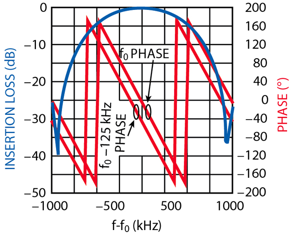
The phase shift requirement is met by controlling the phase in the loop. Assuming that the gain requirement is achieved, the loop will oscillate at the frequency meeting the n x 360° phase shift requirement. Changing the loop phase shift will cause the oscillator to change to a new frequency that provides the n x 360° loop phase shift. The effect of changing the loop phase shift is illustrated in Figure 2 . Note that as the phase shift is increased by 45°, the oscillator shifts to a different frequency that gives a loop phase shift of n x 360° (equivalent to 0°). The frequency is fo - 125 kHz.
VCO Block Diagram
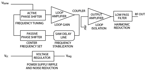
A block diagram of a VCSO is shown in Figure 3 . The VCO incorporates the transmission oscillator and an output amplifier used to isolate the oscillator from external influences. The oscillator loop consists of a SAW delay line, a passive phase shifter, an active phase shifter, a loop amplifier and a directional coupler.
The delay lines are typical of the one shown previously. The delays (δ d ) used range between 0.3 and 1.5 ms, depending upon the tuning range and modulation bandwidth specified. The delay line is designed such that the -3 dB bandwidth is approximately equal to 1/δ d to assure that the phase shift over the SAW delay line bandwidth is single valued.
The phase noise performance is generally an important characteristic of SAW oscillators. The best phase noise performance will be achieved using the longest delay (highest Q) and lowest insertion loss delay line design. However, this conflicts with wide tuning range and high modulation bandwidth. As in most designs, a compromise must be made. A general rule is to make the delay line bandwidth at least twice the required tuning range. This allows for center frequency adjustment and a guard band to prevent "wrap around." The oscillator cannot distinguish between n x 360° and (n+1) x 360°. When the oscillator frequency approaches the -3 dB frequency at one edge of the SAW delay line response, it will jump to the -3 dB frequency of the other band edge. This frequency discontinuity, or wrap around, must be avoided.
All oscillator delay lines are built on a quartz substrate. The frequency temperature coefficient of the quartz delay line is -0.03(T-T0 )2 ppm. This characteristic is a negative parabolic function with the inflection point at T0 . T0 is determined by the cut of the quartz crystal. In most cases, it is desirable to have the VCO inflection point at +25°C, or at the center of the operating temperature range, to minimize the frequency variation due to temperature.
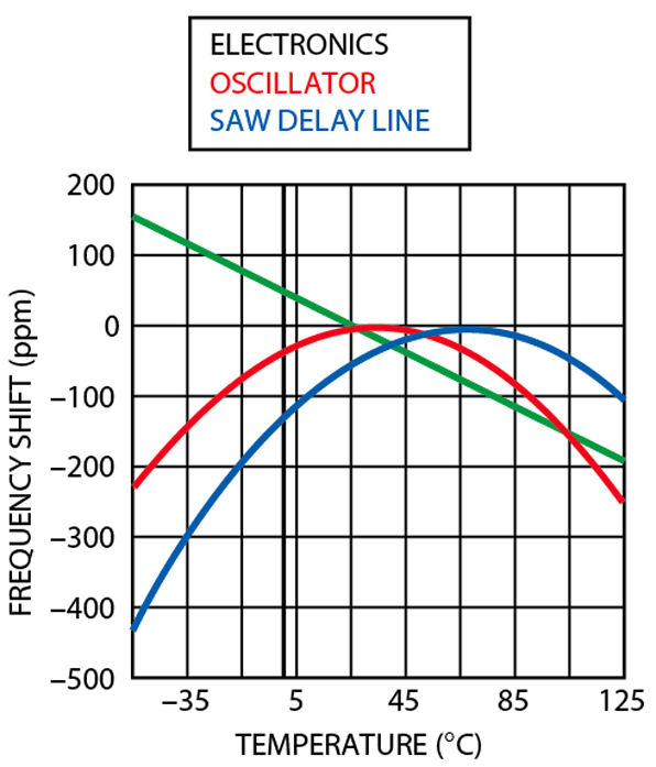
The electronic components of a VCO have a nearly linear phase versus temperature characteristic with a negative slope. The linear phase shift added to the parabolic SAW characteristic results in a parabola having a lower temperature inflection point. The cut of quartz used for the delay line can be varied to change the inflection point. Thus, if the temperature characteristic of the electronic circuitry is known, the correct cut of quartz can be selected for optimum temperature stability. The delay line and oscillator temperature performance are illustrated in Figure 4 .
A passive phase shifter that allows the oscillator center frequency to be set during alignment follows the SAW delay line. The phase shift adjustment is necessary to compensate for variations in insertion phase of other loop components. The adjustment is made using "select-at-test" capacitors.
The active phase shifter provides the voltage-controlled tuning of the oscillator. The active phase shifter is similar in design to the passive phase shifter. The "select-at-test" capacitors are replaced by varactor diodes. The phase shifter provides approximately 180° of linear phase shift.
Both phase shifters are low insertion loss (2 dB) 50 Ω functional blocks. The values of the components used in the phase shifters are easily calculated for any oscillator frequency. Simple value changes allow the same design to function over the entire range of VCSO frequencies.
The loop amplifier provides a gain greater than the total loop insertion loss. In general, 6 to 10 dB of excess gain is desirable to allow for gain changes over the operating temperature range. The amplifier should be selected for the lowest noise figure possible, and an output power level to provide a +10 dBm input to the SAW delay line.
The amplifier phase shift as a function of temperature is important due to its effect on oscillator frequency stability. Most amplifiers are quite good when operated in their linear region. However, when used in a VCO, the amplifier is saturated. Since the phase shift data is rarely provided on a data sheet, the amplifier to be used must be characterized as part of the oscillator design.
Both MMIC RF amplifiers and discrete transistor amplifiers can be used. The MMIC amplifiers require little design effort and are space efficient. However, discrete transistor amplifiers are much more power efficient and allow the design to be optimized for a low power application.
A directional coupler is used to couple out of the loop. Couplings between 3 and 10 dB are used depending upon the oscillator loop insertion loss and the output power requirements.
The output amplifier is needed to isolate the oscillator loop and provide the necessary output power. Low pass filtering is incorporated in the output amplifier to reduce harmonic levels. When digital outputs are required, an appropriate logic interface circuit replaces the amplifier, and the filter is eliminated.
A low noise voltage regulator is used in most VCSOs. The regulator suppresses the external power supply ripple and noise, and provides frequency pushing of less than 2 ppm/V of power supply variation.
Phase Noise
The low noise provided by VCSOs is one of the parameters that dictate their use in many applications. Although achieving low noise performance requires careful design and implementation, understanding and predicting phase noise performance is possible using just a few equations and oscillator parameters.
The first, and simplest, parameter to analyze is the noise floor. The noise floor of an oscillator is the ultimate white noise level, which the oscillator reaches at offset frequencies (f) outside the resonator bandwidth. It is a function of amplifier noise figure, amplifier output power and oscillator loop insertion loss. The noise floor can be calculated as shown below:
Noise floor (dBc/Hz) = KNF = 10log(kT/2) + ILSAW + ILCOUP + ILPS + NFAMP - P0AMP (1)
where
10log = SSB thermal noise (kT/2) in a 1 Hz bandwidth (-177 dBm/Hz)
ILSAW = SAW delay line insertion loss in dB
ILCOUP = coupler loss in dB
ILPS = insertion loss of active and passive phase shifters in dB
NFAMP = amplifier noise figure in dB
P0AMP = amplifier ouptut power in dBm
The calculation for a typical 500 MHz VCSO is
KNF = -177 + 15 + 1 + 4 + 3 - 10 = -164 dBc/Hz (2)
Equation 1 shows the circuit parameters that must be considered in the design of a low noise SAW oscillator. The insertion losses in the loop, including the SAW delay line, must be minimized. A low noise amplifier having as high an output power as is practical should be used. The power is ultimately limited by the SAW delay line. Power levels below 15 dBm can be considered safe for most delay lines.
Once the noise floor has been determined, the phase noise as a function of offset frequency can be calculated. Only two additional oscillator parameters are required for the calculation. The oscillator Q is simply the center frequency divided by the SAW delay line -3 dB bandwidth (f0 /BW). The 1/f or flicker noise corner frequency, fc , is a characteristic of the loop amplifier or the delay line. In the case of SAW delay lines, the amplifier corner frequency dominates. The flicker noise adds an additional 10 dB per decade slope to the phase noise below the corner frequency. An empirical value of 4 kHz for the corner frequency has been determined for silicon bipolar transistors and MMIC amplifiers.
The equation for calculating the single-sideband (SSB) phase noise as a function of offset frequency, fm , is
 (fm ) = (10K NF/10 )[1+(F0 /(2fm Q))2 ](1 + fc /fm ) (3)
Converting to dBc/Hz
(fm )dB = 10log (fm )
where
KNF = noise floor in dBm/Hz
F0 = oscillator output frequency
fm = offset frequency
Q = oscillator quality factor (f0 /BW)
fc = 1/f noise corner frequency
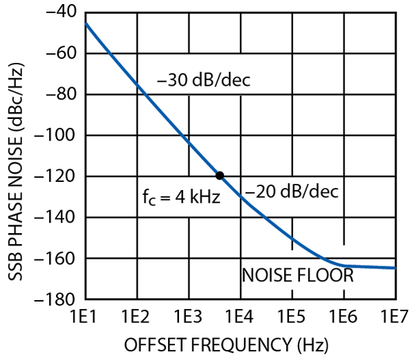
Figure 5 shows a plot of the calculated phase noise for a 500 MHz VSCO having a 1 MHz bandwidth, -165 dBm noise floor and a 1/f noise corner frequency of 4 kHz. Note that the noise rises from the noise floor at a 20 dB/decade slope and changes to 30 dB/decade at fc . Changes in the noise floor simply shift the entire phase noise curve either up or down.
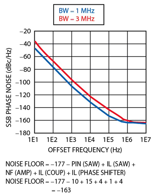
Figure 6 illustrates the effect of changing the delay line bandwidth. Note that, with all other parameters remaining unchanged, increasing the delay line bandwidth from 1 to 3 MHz increases the phase noise by 10 dB.
VCSO Applications
Historically, VCSOs were built as discrete hybrid modules with a typical footprint of 1.0" x 1.5". New technology has made it possible to integrate ASICs and SAW technology to produce high performance VCSOs in small ceramic surface-mount packages.
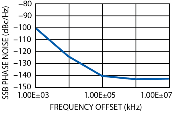
These VCSOs find large use in telecom applications such as low jitter clocks. A typical SSB phase noise for this type of VCSO having low voltage positive emitter coupled logic (LVPECL) outputs is shown in Figure 7 .
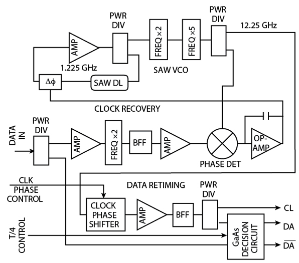
VCSOs find application in high performance synchronous optical networks (SONET) and 10GE clock recovery applications. The clock data recovery circuits (CDR) use a frequency multiplied VCSO in a phase-lock loop (PLL) as a tracking filter to recover a low jitter clock from the incoming non return to zero (NRZ) data stream.
The PLL loop bandwidth can be adjusted between 0.1 and 6 MHz to optimize jitter performance. The data is retimed by a high performance GaAs decision circuit. A block diagram of a VCSO-based CDR is shown in Figure 8.
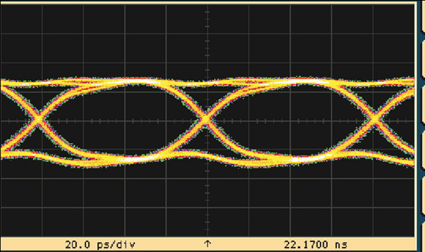
An eye diagram at the OC-192 CDR data output with a 231-1 pseudorandom bit sequence (PRBS) is shown in Figure 9.
Conclusion
The information presented in this article provides insight into the operation of a VCSO. Critical performance parameters and the design parameters affecting them have been discussed. In addition, two applications that make use of VCSO technology to provide high performance telecom solutions have been presented.
References
1. M.F. Lewis, "Some Aspects of SAW Oscillators," 1973 Ultrasonics Symposium Proceedings , pp. 344-347.
2. W.P. Robins, Phase Noise in Signal Sources , Peter Peregrinus Ltd., London, UK, 1982.
3. A. Hajimiri and T. Lee, "A General Theory of Phase Noise in Electrical Oscillators," IEEE Journal of Solid State Circuits , February 1998, pp. 179-194.