
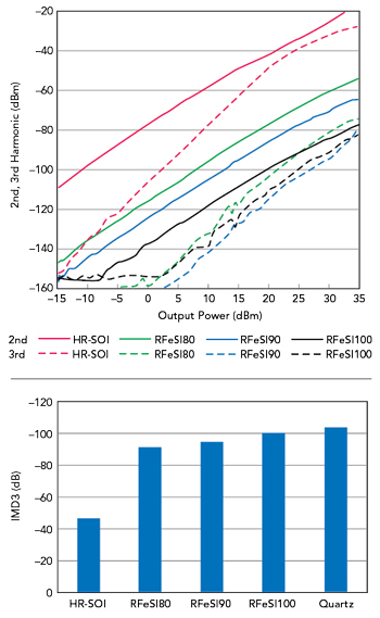
Figure 1 RF-SOI substrate second and third harmonics (a) and 845 MHz IMD3 (b).
5G and Wi-Fi 6(E) are creating new user experiences that require unprecedented network capacity with on-demand data throughput at record low latencies. To address these requirements, spectral resources from 100s of MHz to mmWave frequencies have been assigned to these standards. Gbps data rates are offered at these bands using record high waveform complexity, tightening RFIC linearity specifications to minimize signal distortion.
Over the last two decades, silicon on insulator (SOI) has proven to be the semiconductor solution of choice for highly linear, power efficient, integrated wireless systems. At the same time, the world’s near to endless CMOS capacity and the demonstrated large-scale manufacturability of RF-SOI substrates have enabled cost effective solutions for 4G/LTE and Wi-Fi. Today, 5G and Wi-Fi 6(E) are benefiting from this demonstrated capability. This article reviews the continuous innovation of SOI engineered substrates to address the challenges of today’s and future wireless systems.
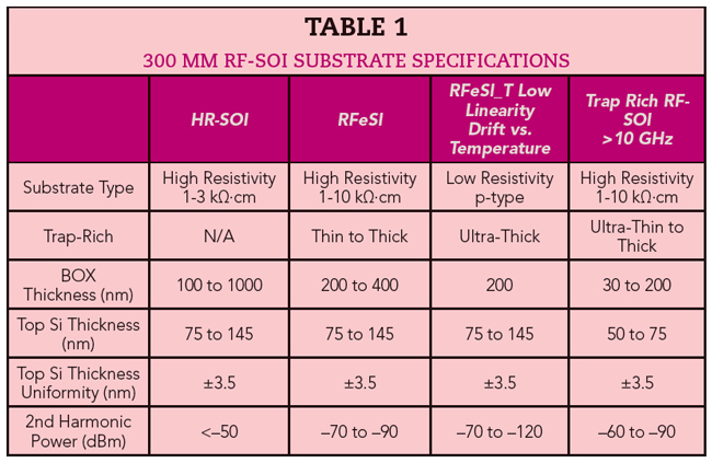
HR-SOI to TRAP-RICH SOI
Compared to bulk silicon technology, SOI’s key advantages for RF applications have led to its general adoption in smartphone front-end modules over the past decade, spearheaded by RF switches. SOI wafers are composed of a thin silicon layer, usually 50 to 150 nm where the active devices are built, fully isolated from the underlying or “handle” wafer by a buried oxide (BOX) layer.
This configuration has major benefits. First, the shallow trench isolation reaches the BOX and effectively eliminates any conduction path between devices. This, in turn, enables transistor stacking to a level unsustainable using junction isolation. It also drastically improves the isolation between circuit blocks. The second benefit is the ability to engineer the handle wafer specifically for communication applications without degrading the quality of the active device layer, leading to high resistivity (HR) silicon being implemented as the handle wafer material. Decreasing the concentration of free carriers in the handle wafer reduces the attenuation or insertion loss (IL) of the propagated signal, resulting in better power transmission efficiency. It also reduces the power of the parasitic signals generated at the harmonic frequencies of the carrier signal, i.e., harmonic distortion (HD) or, when multiple signals are involved, intermodulation distortion (IMD).
Though the HR handle is highly beneficial, the HR-SOI wafer has an inherent capacitor-like configuration, which results in the possible creation of a low resistivity, free carrier accumulation or inversion layer underneath the BOX, dubbed the parasitic surface conduction (PSC) layer.1 This issue can be circumvented with an engineered layer between the BOX and HR handle containing a high density of electrically active traps.2,3 Three game-changing effects of this trap-rich (TR) layer are the Fermi level pinning induced by the traps, the trapping of free carriers from the base wafer and the reduction of mobility. A higher level of signal fidelity can be achieved: the isolation is improved because the conductive coupling below the BOX is suppressed, leaving only capacitive coupling. The fluctuation of carrier concentration below the BOX is suppressed, as the Fermi level is pinned close to the middle of the semiconductor’s gap, linearizing the handle’s resistance and capacitance and drastically reducing HD. Finally, the constant HR further reduces IL.
The following section discusses Soitec’s TR SOI family of substrates and how the RF performance compares to HR-SOI for different wireless applications (see Table 1). The measurements shown throughout the article, unless otherwise stated, are performed on 2.1 mm long coplanar waveguide (CPW) at a fundamental frequency of 900 MHz. The DC bias refers to the bias applied between the central line and ground lines; the latter connected to the substrate backside. The second harmonic power levels are referenced to a fundamental frequency output power of 15 dBm at a default DC bias of 0 V.
RF-SOI SUBSTRATES for RF FRONT-ENDS
Depending on the intended function in the RF front-end (RFFE), the diverse RF circuits impose different requirements on the RF-SOI substrate, i.e., for large signal (linearity, power handling) or small signal and immunity to interferers (crosstalk, digital noise).4–6 Given the increasing complexity of the RFFE, high density integration of digital logic, memory and RF functions must also be carefully considered. The final system application - such as infrastructure or mobile user equipment (UE) - will also dictate specifications including ruggedness and robustness.
Large-signal switching, shaping and amplification can introduce signal distortion because of the inherent nonlinear nature of active RF circuits. Soitec’s RFeSI™ substrates help minimize distortion by reducing parasitics, as previously explained. Figure 1 shows the harmonic and intermodulation products generated on three RFeSI TR SOI substrates with guaranteed second harmonic power below ‐100 dBm (RFeSI100), ‐90 dBm (RFeSI90) and ‐80 dBm (RFeSI80). The IMD performance is measured with two 20 dBm tones at 900 and 955 MHz.7
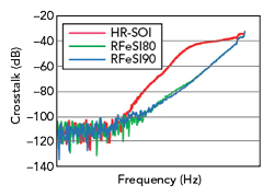
Figure 2 RF-SOI substrate crosstalk immunity.
The complexity of the digital and control content of the RFFE has been steadily increasing. For example, several 26 MHz - up to 52 MHz - MIPI RFFESM bus instances are required to control the radios in the modern smartphone, including 5G, Wi-Fi, Bluetooth, GNSS and NFC. Even with the complexity, the control and digital signals must not interfere with the RF and vice versa. A good RF substrate should help prevent unwanted signals conducting from one part of the system to another - whether control, digital or RF - as they can disrupt system operation. Crosstalk and digital noise immunity are very important when designing RF and mmWave front-ends, and the design starts with the substrate (see Figure 2).5