

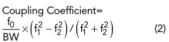
Once the coupling matrix is obtained, geometric modeling starts. Two identical resonators with different coupling schemes are shown in Figure 5. For this design, the iris coupling scheme with a blind hole is used to control the main coupling parameters. By adjusting the depth of the hole keeping the iris width fixed, different coupling strengths can be obtained. The blind hole coupling scheme is employed to realize the transmission zeros by means of in and out of phase variation. The coupling coefficient is calculated using Equation 2,7 where f1 and f2 are the even and odd mode resonant frequencies, respectively. These values can be obtained by using the HFSS eigenmode solver.
By tuning slot length, blind hole depth or through-hole distance, a wide range of coupling coefficients can be achieved. Table 2 summarizes the properties, advantages and disadvantages of each cavity coupling scheme.

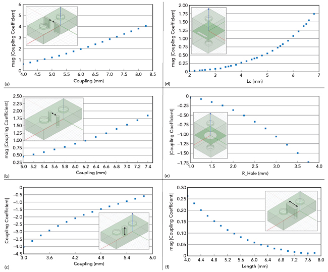
Figure 5 Coupling coefficient magnitude contours for iris (a), through hole (b), blind hole (c), slot (d), slot (e) and iris (f) coupling.
The input and output structures use coaxial pins to excite the TE101 mode. By varying pin depth and its position, different input/output coupling strengths can be obtained. During the optimization process, the blind hole depth on top of each cavity, serving as the tuning screw, must be fine-tuned to compensate for frequency variation caused by the coaxial pin’s loading effect. Figure 6 shows the final simulated result.
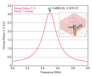
Figure 6 Simulated group delay vs. frequency, with 3D view, of the optimized design.
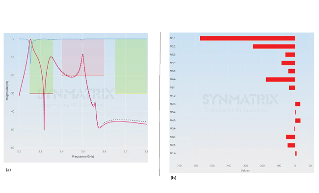
Figure 7 Initial simulated result (dotted line) vs. extracted performance (solid line) for the full 3D structure (a) and coupling bandwidth extracted error (b).
3D Analysis and Simulation
To compensate for loading effects resulting from the input and output structures, the first and the last cavity lengths are shortened slightly. All critical dimensions obtained from the previous simulation are applied to the full 3D structure construction. Initial performance and corresponding error information are shown in Figure 7.
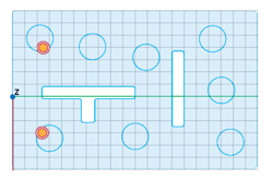
Figure 8 HFSS layout showing the open windows used to control the transmission zeros.
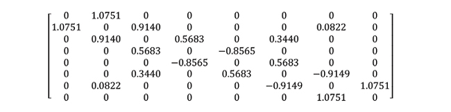
To make the manufacturing process easier and avoid crack risks during mold development, the coupling coefficient signs for M12 and M34 (realized by a blind hole) are changed without any impact to performance. The transmission zeros controlled by M2,5 and M1,6 can be easily achieved by varying the open windows without any extra tuning mechanism as shown in Figure 8. The final product benefits from a more stable manufacturing process by lowering the crack issue risk during the pressing and sintering process. The new coupling matrix is:
After several rounds of optimization, final performance is achieved. During optimization, the matrix extraction technique is used. Importing the simulated S2P file each time enables a steady and accurate optimization process.
MEASUREMENTS
Figure 9a shows the final simulation results and Figure 9b shows the correlation between simulation and measurement. All coupling errors are controlled within 1 percent. The extracted unloaded Q is about 2,020 compared to the target value of 2,000. Thermal drift value is around 0.65 MHz within the operating temperature range. Additionally, since the first and last resonator sizes are reduced due to the input and output coupling loading effect, the first spurious is pushed to 5.3 GHz. Unbalanced notch performance is caused by stray energy leakage affecting M2,4 and M1,5.
Figure 10 shows the fabricated filter (the surface is silver plated). The total length is 40 mm, the width is 26 mm and the height including the SMA connector is 15.5 mm. Due to material property variation, the final prototype is fine-tuned by grinding and replating the blind holes for M1,1, M2,2 and M5,5 to help compensate for return loss variation.
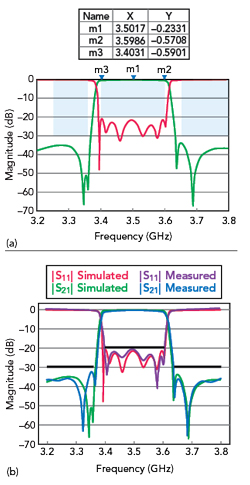
Figure 9 Simulated (a) and measured vs. simulated (b) performance of the filter.
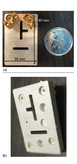
Figure 10 Top (a) and side (b) views of the ceramic waveguide filter.
CONCLUSION
A procedure for designing a dielectric-filled waveguide filter starts with an unloaded Q analysis followed by a specification analysis that considers material selection, temperature drift and topology (which relates to the practical mechanical design). Given the material, the coupling matrix is synthesized with margins based on design specifications. Q analysis (based on a single cavity) and a comparison of cavity coupling schemes and input/output structures are discussed. The results of 3D model simulation and optimization show excellent correlation with measurements.
References
- K. Sano and M. Miyashita, “Dielectric Waveguide Filter with Low Profile and Low-Insertion Loss,” IEEE Transactions on Microwave Theory and Techniques, Vol. 47, No. 12, December 1999, pp. 2299–2303.
- Y. Konishi, “Novel Dielectric Waveguide Components - Microwave Applications of New Ceramic Materials,” IEEE Proceedings, Vol. 79, No. 6, June 1991, pp. 726–740.
- S. Afridi, I. Hunter and M. Y. Sandhu, “Spurious Free Non Uniform Width Dielectric Loaded Filters,” European Microwave Conference, September 2018.
- D. M. Pozar, Microwave Engineering, 2012.
- “3D Electromagnetic Field Simulator for RF and Wireless Design,” Ansys, Web. www.ansys.com/Products/Electronics/ANSYS-HFSS.
- SynMatrix Technologies Inc., Web. www.synmatrixtech.com.
- R. J. Cameron, C. M. Kudsia and R. R. Mansour, “Microwave Filters for Communication Systems: Fundamentals, Design, and Applications,” Wiley, 2007.